
Mindmap
PV 2
Inhalt der Mindmap
PV 2
RECAP PV1
- electron / hole pair generation
- photon = absorbed - electron goes from VB to CB
- hole left in VB - electron hole pair
- photon = absorbed - electron goes from VB to CB
- indirect band gap
- complex - decreases absorption efficiency
- electron / hole pair generation
Electron - hole annhilation
- three methods
- Auger
- Three carrier process
- Electron/hole recombine
- dont emit heat / photon - give enrgy to a third carrier = electron in conduction band
- electron rasies up energy levels in conduction band, then thermalizes back down to CB edge
- dont emit heat / photon - give enrgy to a third carrier = electron in conduction band
- Electron/hole recombine
- Three carrier process
- Radiative
- band - band recombination
- electron from CB combines with Hole from VB
- releases photon - photon energy approx that of band gap so can exit
- dominates in direct band gap semi conductors
- electron from CB combines with Hole from VB
- band - band recombination
- SRH (Schokly-Read-Hall)
- "defects recombination"
- does not occur in pure undefected material
- two step process
- electron drops from CB to a energy state in the "forbidden" region
- level introduced because of material defects
- hole moves up to the same energy state before the electron is thermally re-emitted into conduction band = recombines
- level introduced because of material defects
- electron drops from CB to a energy state in the "forbidden" region
- "defects recombination"
- Auger
- three methods
Current generation
- electrons passing across band gap = electric current
- Ip=qNA
- N = fraction of photons in usable region of spectrum
- A= surface area of semiconductor exposed to light
- Ip=qNA
- light induced current generates a voltage
- electric power is generated by separating the electrons and holes at device terminals
- Vmax=Eg/q
- Vmax = bandgap of semicondcutor in eV
- Vmax=Eg/q
- electric power is generated by separating the electrons and holes at device terminals
- electrons passing across band gap = electric current
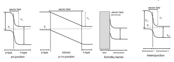
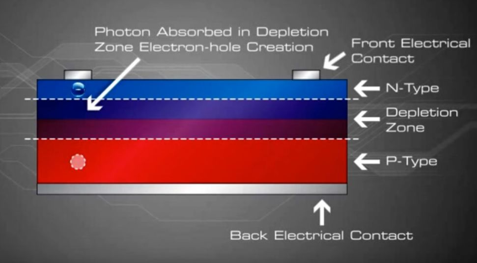
creating a semiconductor junction
- 4 main types
- PN
- PIN
- Schottky Barrier
- Heterojunction
- each has a built in potential
- Junction generates strong electric fields
- between two semiconductors
- n-type electrons near interface cross to p-type side = leave a positively charged area
- P-type holes transfer to n-type side = leaves a negatively charged area
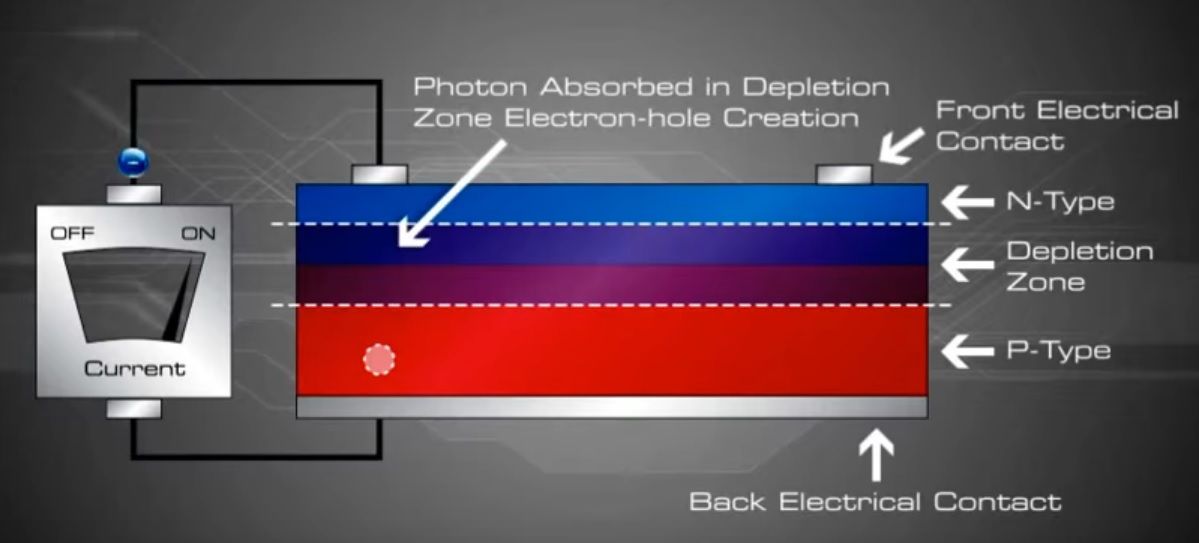
- creates a depletion zone - no mobile charges
- prevents flow of electrons / holes
- photon = absorbed
- electron/hole pair from depletion zone
- electron flows into N-type, hole into p-type, flows around circuit
- electron/hole pair from depletion zone
- photon = absorbed
- prevents flow of electrons / holes
- creates a depletion zone - no mobile charges
- P-type holes transfer to n-type side = leaves a negatively charged area
- n-type electrons near interface cross to p-type side = leave a positively charged area
- between two semiconductors
- Biasing junctions
- no net current at equilibrium
- forward bias = reduced barrier height occurs - increases current through diode..
- negative termianl of battery connected to n-type, repulsion pushes electrons towards depletion zone
- Postive termainl replusle the hoels towards the depletion zone
- battery ahs enough power to overcome depletion zone, holes and electons can combine in depletion and create a current
- Postive termainl replusle the hoels towards the depletion zone
- negative termianl of battery connected to n-type, repulsion pushes electrons towards depletion zone
- reverse bias
- draws electrons and holes away from depletion zone, increase depltion zone, prevetns current flow
- 4 main types
how a solar cell works
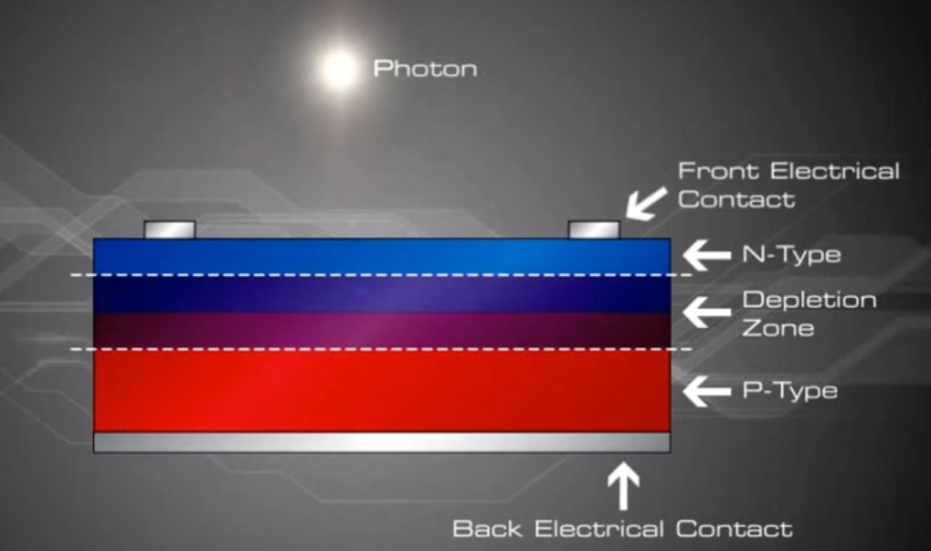
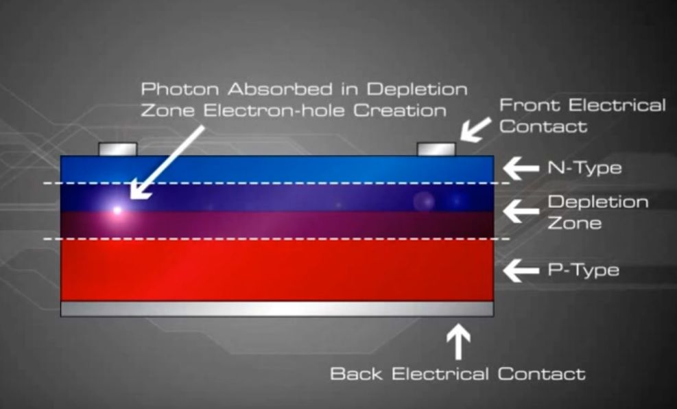
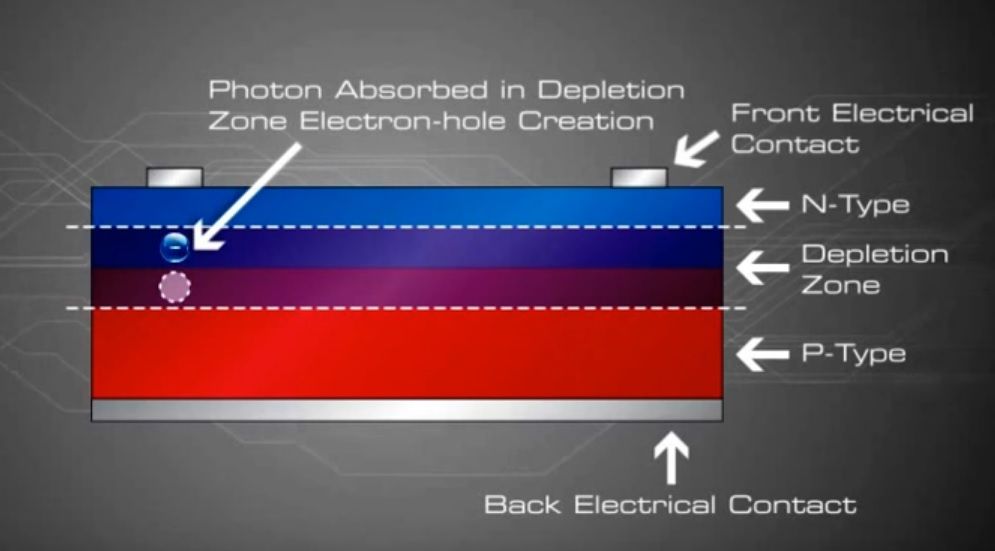
- Photon absorbed
- energy of photon absorbed in depletion zone
- creates a free electron and a hole - enough energy to jump out of the depletion zone
- negative electron is attracted to +ve P type, so flows through n-type, around circuit, into back of p-type where it combines with hole
- creates a free electron and a hole - enough energy to jump out of the depletion zone
- energy of photon absorbed in depletion zone
- Photon absorbed
PN junction under external bias
- Curve properties
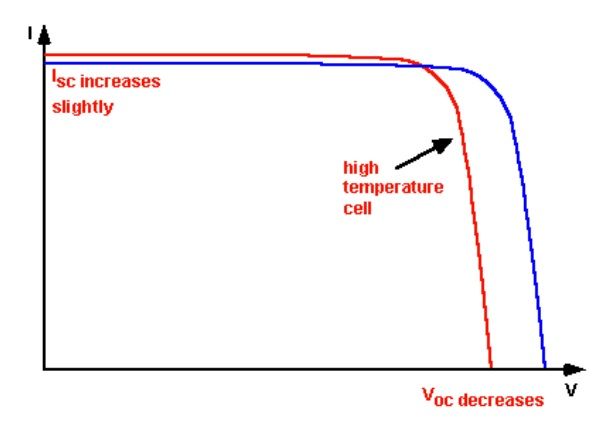
- short-circuit current = Isc
- occurs through solar cell when voltage across teh cell is zero
- Voc - open circuit votlage
- is the maximum votlage available from the cell, occuring at zero current
- Fill factor / small area/ big area
- ff=imp*vmp/Isc&Voc
- solar cell efficiency = Pmax(pout)/Pin = FFVocIsc/Pin
- short-circuit current = Isc
- Temperature effects
- increasing temperature reduces Eg
- viewew as increasing the energy of electrons in semiconductor
- less energy needed to break the bonduing, rduction in bond energy = reduction in band gap
- Voc - affected most by increasing T
- less energy needed to break the bonduing, rduction in bond energy = reduction in band gap
- viewew as increasing the energy of electrons in semiconductor
- increasing temperature reduces Eg
- Curve properties
Bilder und Dateien der Mindmap
Informationen
- Beschreibung
- Mindmap am PV 2, erstellt von Tom Piggott am 26/05/2017.
- Erstellt von
- Tom Piggott
- Aufrufe
- 0
- Bewertung