
Quiz
Field Effect Transistors
Erstelle ein kostenloses Konto, um dieses Quiz zu beenden
Speichere deinen Fortschritt und sieh dir dein Endergebnis an.
oder mit deiner E-Mail registrieren
Schon ein Konto? Anmelden
Fragen in diesem Quiz (32)
1Junction Field Effect Transistors (JFET) contain how many diodes?
- A4
- B3
- C2
- D1
2When an input delta of 2 V produces a transconductance of 1.5 mS, what is the drain current delta?
- A666 mA
- B3 mA
- C0.75 mA
- D0.5 mA
3When not in use, MOSFET pins are kept at the same potential through the use of:
- AShipping foil
- BNonconductive foam
- CConductive foam
- Da wrist strap
4D-MOSFETs are sometimes used in series to construct a cascode high-frequency amplifier to overcome the loss of:
- Alow output impedance
- Bcapacitive reactance
- Chigh input impedance
- Dinductive reactance
5A "U" shaped, opposite-polarity material built near a JFET-channel center is called the:
- Agate
- Bblock
- Cdrain
- Dheat sink
6When testing an n-channel D-MOSFET, resistance G to D = infinity, resistance G to S = infinity, resistance D to SS = and 500 ohms, depending on the polarity of the ohmmeter, and resistance D to S = 500 infinity. What is wrong?
- Ashort D to S
- Bopen G to D
- Copen D to SS
- Dnothing
7In the constant-current region, how will the IDS change in an n-channel JFET?
- AAs VGS decreases ID decreases.
- BAs VGS increases ID increases.
- CAs VGS decreases ID remains constant.
- DAs VGS increases ID remains constant.
8A MOSFET has how many terminals?
- A2 or 3
- B3
- C4
- D3 or 4
9IDSS can be defined as:
- Athe minimum possible drain current
- Bthe maximum possible current with VGS held at –4 V
- Cthe maximum possible current with VGS held at 0 V
- Dthe maximum drain current with the source shorted
10 What is the input impedance of a common-gate configured JFET?
- Avery low
- Blow
- Chigh
- Dvery high
11JFET terminal "legs" are connections to the drain, the gate, and the:
- Achannel
- Bsource
- Csubstrate
- Dcathode
12A very simple bias for D-MOSFET is called:
- Aself biasing
- Bgate biasing
- Czero biasing
- Dvoltage-divider biasing
13With the E-MOSFET, when gate input voltage is zero, drain current is:
- Aat saturation
- Bzero
- CIDSS
- Dwidening the channel
14 With a 30-volt VDD, and an 8-kilohm drain resistor, what is the E-MOSFET Q point voltage, with ID = 3 mA?
- A6 V
- B10 V
- C24 V
- D30 V
15When an input signal reduces the channel size, the process is called:
- Aenhancement
- Bsubstrate connecting
- Cgate charge
- Ddepletion
16Which JFET configuration would connect a high-resistance signal source to a low-resistance load?
- Asource follower
- Bcommon-source
- Ccommon-drain
- Dcommon-gate
17How will electrons flow through a p-channel JFET?
- Afrom source to drain
- Bfrom source to gate
- Cfrom drain to gate
- Dfrom drain to source
18When VGS = 0 V, a JFET is:
- Asaturated
- Ban analog device
- Can open switch
- Dcut off
19When applied input voltage varies the resistance of a channel, the result is called:
- Asaturization
- Bpolarization
- Ccutoff
- Dfield effect
20When is a vertical channel E-MOSFET used?
- Afor high frequencies
- Bfor high voltages
- Cfor high currents
- Dfor high resistances
21When the JFET no longer able to control the current, this point is called the:
- Abreakdown region
- Bdepletion region
- Csaturation point
- Dpinch-off region
22With a JFET, a ratio of output current change against an input voltage is called:
- Atransconductance
- Bsiemens
- Cresistivity
- Dgain
23Which type of JFET bias requires a negative supply voltage?
- Afeedback
- Bsource
- Cgate
- Dvoltage divider
24How will a D-MOSFET input impedance change with signal frequency?
- AAs frequency increases input impedance increases.
- BAs frequency increases input impedance is constant.
- CAs frequency decreases input impedance increases.
- DAs frequency decreases input impedance is constant.
25The type of bias most often used with E-MOSFET circuits is:
- Aconstant current
- Bdrain-feedback
- Cvoltage divider
- Dzero biasing
26The transconductance curve of a JFET is a graph of:
- AIS versus VDS
- BIC versus VCE
- CID versus VGS
- DID x RDS
27The common-source JFET amplifier has:
- Aa very high input impedance and a relatively low voltage gain
- Ba high input impedance and a very high voltage gain
- Ca high input impedance and a voltage gain less than 1
- Dno voltage gain
28Using voltage-divider biasing, what is the voltage at the VGS?
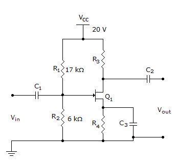
- A5.2 V
- B4.2 V
- C3.2 V
- D2.2 V
29The overall input capacitance of a dual-gate D-MOSFET is lower because the devices are usually connected:
- Ain parallel
- Bwith separate insulation
- Cwith separate inputs
- Din series
30What is the transconductance of an FET when delta ID = 1 mA and delta VGS = 1 V?
- A1 kS
- B1 mS
- C1 kiloohm
- D1 milliohm
31Which component is considered to be an "OFF" device?
- Atransistor
- BJFET
- CD-MOSFET
- DE-MOSFET
32In an n-channel JFET, what will happen at the pinch-off voltage?
- AThe value of VDS at which further increases in VDS will cause no further increases in ID.
- BThe value of VGS at which further decreases in VGS will cause no further increases in ID.
- CThe value of VDG at which further decreases in VDG will cause no further increases in ID.
- DThe value of VDS at which further increases in VGS will cause no further increases in ID
Informationen
- Beschreibung
- II Engineering Electronics II Quiz am Field Effect Transistors, erstellt von Tony Mae am 06/03/2021.
- Autor
- Tony Mae
- Sprache
- English
- Aufrufe
- 25
- Schlagwörter
- Bewertung
- Noch keine Bewertungen Bewerte dieses Quiz