
Test
savethehell
Crea una cuenta gratis para terminar este test
Guarda tu progreso y consulta tu resultado final.
¿Ya tienes cuenta? Inicia sesión
Preguntas del test (80)
1Diagram of an electronic power supply is presented in figure. Define why is using a voltage regulator in rectifier circuits.
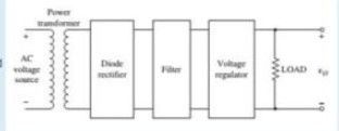
- AIt absorbs a constant voltage level
- BIt maintans a constant voltage level
- CIt generates a constant voltage level
2To limit output voltage of positive limiter to 5V, when a 10V peak input voltage is applied, bias voltage must be:
- A4.3V
- B0.7V
- C3.4V
- D3V
3PIV is which of the following?
- Apositive input voltage
- Bpeak inverse voltage
- Cpeak input voltage
- Dpeak immediate voltage
4A p-n junction diode is under various battery supply connection is shown in Figure. Show the figure, which illustrates a diode inder reverse bias.
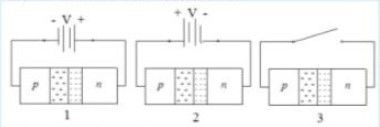
- A1
- B2
- C3
5Define what is rectifier?
- ADevice which converts dc voltage into an alternating (ac) voltage
- BDevice which generates dc voltage
- CDevice which converts alternating (ac) voltage into an dc voltage
6At using of such rectifier the time diagram of output voltage will be:
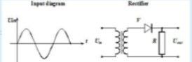
- A
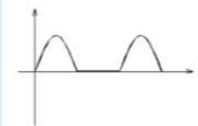
- Banother
- Canotherr
- A
7If a zener diode has 25 volts across it and 20mA of current flowing through it, what is the zener diode power dissipation?
- A3W
- B4W
- C5W
8The minority carriers in p-type semiconductor
- Aions
- Bholes
- Celectrons
9What type of diode circuit is used to add or restore a dc level to an electrical signal?
- Aclamper
- Bnone of the above
- Cclipper or limiter
- DIC voltage regulator
10Identify which part of the diode shown in figure is P materian and which part is N material:

- AThe anode is N material, the cathode is P material
- BThe anode is PN material, the cathode is PN material
- CThe anode is P material, the cathode is N material
11What is the relationship between depletion width and the concentration of impurities?
- AIncrease in doping decreases the width of depletion layer
- BDecrease in doping increases the width of depletion layer
- CThe magnitude of N-type and P-type doping set the depletion layer
12In the shown figure are represented PN junction diode symbols. Identify the unknown stripe
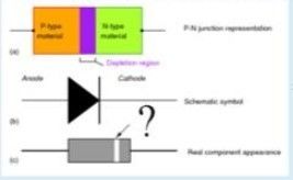
- ACathode
- BAnode
- CDepletion region
13The simplest half-wave circuit of rectification is
- A
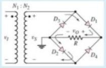
- B
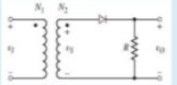
- C
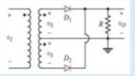
- A
14The breakdown voltage is often called the peak inverse voltage (PIV) or the peak reverse voltage (PRV). Following are the PIVs of some common diodes. Which can permanently destroy a diode, excessive current or excessive voltage?
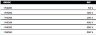
- AExcessive current. Excessive voltage will not harm the diode if the current is limited
- BNo one
- CExcessive voltage. Excessive current will not harm the diode if the current is limited
15A p-n junction diode is under various battery supply connection is shown in Figure. Show the figure, which illustrates a diode under forward bias.
- A1
- B2
- C3
16What is the charge carriers in P-type?
- Aimmobile ions
- Bholes
- Celectrons
17Explain the given I-V curve
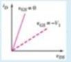
- Aa small reverse-biased gate voltage
- Bzero gate voltage
- Ca gate voltage that achieves pinchoff
18Identify the correct statement for a given Figure

- AThe lamp sometimes on, sometimes off
- BThe lamp is off
- CThe lamp is on
19Refer to FIG if input B is more positive than input A, which diodes will be conducting?
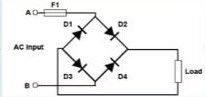
- AD1 and D2
- BD3 and D4
- CD2 and D3
- DD1 and D4
20From the illustrations below, select the parallel negative limiter with positive bias
- A

- B

- C

- D

- A
21The dc current through each forward-biased diode in a full-wave rectifier equals
- AHalf the dc load current
- BThe load current
- CTwice the dc load current
22Under what condition depletion layer thickness is charged?
- Awhen a p-n junction is heavily doped
- Bwhen a p-n junction is lightly doped
- Cwhen an external voltage is applied to a p-n junction
23From the illustrations below, select the series negative limiter
- A
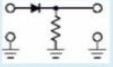
- Bсмотри на стрелку
- A
24Which statement is true for a forward biased diode?
- AForward bias will eliminate the depletion zone and cause a diode to pass current
- BDue to the massive electron flow, normal PN junction diodes are destroyed when operated in this manner
- CThe positive potential on the cathode will atract electrones from the depletion zone.
25What is the action of the reservior capacitor in a basic power supply
- ATo decrease the DC component and reduce the AC component of the AC wave
- BTo remove the DC component of the AC wave
26The most widely used rectifier is
- Ahalf-wave rectifier
- Bfull-wave bridge rectifier
- Cfull-wave center-tapped rectifier
27Which of the following could be used as donor atom to produce P-type semiconductor material
- ABoron
- BCarbon
- CPhosphorus
28Sketch the output diagram of the given circuit if the input diagram...
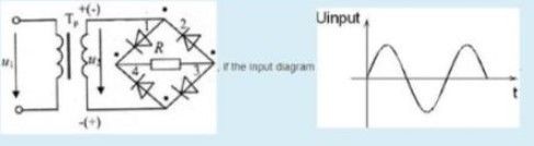
- A
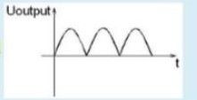
- B
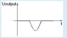
- C
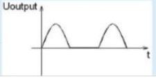
- A
29What is intrinsic semiconductor?
- Athe densities of holes and electrons are equal
- Bthe densities of electrons are less than holes
- Cthe densities of electrons are more than holes
30When the leakage current only becomes series?
- Awhen the diodes reverse voltage reaches breakdown, which causes an avalanche of current to flow
- Bthe resistant potential barrier is increased which prevents the flow of majority carriers in both directions
- Cwhen the potential barrier at the junction completely dissapears and hence, the holes cross the junction from P to N type and electrons cross the junction to opposite direction...........
31Intrinsic semiconductor material is charachterized by a valence shell of how many electrones?
- A3
- B4
- C2
32When a current flows through a diode, it causes heating and power dissipation, just
as with a resistor. The power formula for resistors is P 5 V 3 I. This same formula can be
applied to diodes to find the power dissipation.
To calculate the power dissipation in a diode, you must first calculate the current as
shown previously. The voltage drop in this formula is assumed to be 0.7 volt for a silicon
diode, even if you considered it to be 0 volts when calculating the current.
For example, a silicon diode has 100 mA flowing through it. Determine how much
power the diode dissipates.- A60
- B80
- C70
33What happens to the current when the voltage becomes limited at the knee?
- AIt is not change
- BIt increases rapidly
- CIt decreases rapidly
34Define a zero bias p-n junction
- Awhen an internal voltage is applied
- Bwhen no external voltage is applied
- Cwhen an external voltage is applied
35During positive half-cycle of total secondary voltage of bridge rectifier, number of diodes forward biased are
- Atwo
- Bthree
- Cfour
- Done
36In PNP transistors, the flow from emitter to collector is composed of ________
- AElectrons
- BHoles
- CIons
37_________ is a break-up of covalent bond to form electron and hole pairs
- Ainjection
- Bgeneration
- Crecombination
38______________ is formed by joining p_type and N-type semiconductors together in very close contact
- Aphase transition
- BPN Junction
39Define what is a full-wave rectifier circuit?
- Aa rectified output voltage occurs during both the positive and negative cycles of the input signal
- Ba rectified the output voltage appears only during the positive cycle of the input signal
- Ca rectified the output voltage appears only during the negative cycle of the input signal
40When a diode is in its non-conducting state it has
- Aa very high resistance
- Ba very low resistance
- Cno resistance at all
41When semiconductor is doped half with trivalent and half with pentavalent impurities, junction formed is known as
- Abarrier junction
- BP-N junction
- Cpotential barrier
42Why doping is done in semiconductors?
- Afor improvement of a chemical property
- Bto change a crystallic structure
- Cto increase an electrical conductivity
43Which statement is true for the leakage current
- AIn case of leakage current, temperature plays an important role. The minority current are mostly temperature dependent
- BGenerally leakage current is so high
- CIn Germanium and Silicon diodes, leakage current is Mega amperes and Kilo amperes, respectively
44Define what is a half-rectifier circuit?
- Aa rectified output voltage occurs during both the positive and negative cycles of the input signal
- Ba rectified the output voltage appears only during the positive cycle of the input signal
- Ca rectified the output voltage appears only during the negative cycle of the input signal
45What happens to the diode resistance at the limiting or knee voltage?
- AIt is not change
- BIt changes from low to high
- CIt changes from high to low
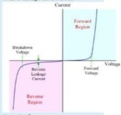
46What is leakage current diode depend on?
- ALeakage current is dependent on electrons and holes
- BLeakage current is dependent on minority current carriers
- CLeakage current is dependent on majority current carriers
47Zener diodes are also known as
- AReverse bias diode
- BForward bias diode
- CNone of the mentioned
- DBreakdown diode
48When semiconductor is under forward bias condition, width depletion
- Aincreases
- Bdoesn't change
- Cdecreases
49What is the function of a limiter circuit?
- ALimit the Amplitude of any waveform to predetermined level
- BMaintain the reference level at a constant value
- CLimit the Frequency to a predetemined value
- DRegulate the DC Voltage output level
50As the forward voltage increased for Vf < V0 why in the VI curve the forward current If almost zero?
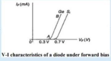
- Abecause the potential barrier in the forward bias increases
- Bbecause the potential barrier prevents the holes from P region and electrons from N region to flow across the depletion region in opposite direction
- C*the longest answer*
51The cut in voltage or threshold voltage Vf below which the current is very small. At this voltage the potential barrier is overcome and the current through the junction starts to increase rapidly as shown in Figure. Explain why it happens
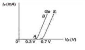
- Abecause the potential barrier at the junction completely dissappears and hence, the holes cross the junction from P to N type and electronics cross the junction to opposite direction, resulting large current flow in external circuit.
- Bbecause the potential barrier in the forward bias increases.
- Cbecause the potential barrier prevents the holes from P region and electrones from N region to flow across the depletion region in opposite direction.
52The region in a semiconductor diode where no free charge carriers exists is known as the
- Aanode region
- Bcathode region
- Cdepletion region
53Calculate the current through the diode
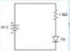
- A10mA
- B9.5mA
- C9mA
54When the diode is connected so that the current is flowing. It is said to be forward biased. Examine the way the diode is connected to the battery in Figure.

- AYes. But the cathode is connected to the positive battery terminal and the anode is connected to the negative battery terminal. Therefore, the anode is at a lower voltage than the cathode.
- BYes. The anode is connected to the positive battery terminal, and the cathode is connected to the negaive battery terminal. Therefore, the anode is at a higher voltage than the cathode.
- CNo, it is not forward biased. The cathode is connected to the positive battery terminal and the anode is connected to the negative battery terminal. Therefore, the cathode is at a higher voltage than the anode.
55Rectifier which results an output with a frequency that pulsates every half cycle of input voltage is
- Afull wave rectifier
- Bhalf wave rectifier
- Cmodulator
- Dregulator
56In the circuit shown in figure an arrow shows the direction of current. Is the diode conected correctly to permit current to flow? And notice the way the battery and the diode are connected. Is the anode at a higher or lower voltage than the cathode?

- AYes. But the cathode is connected to the positive battery terminal and the anode is connected to the negative battery terminal. Therefore, the anode is at a lower voltage than the cathode.
- BNo. The cathode is connected to the positive battery terminal and the anode is connected to the negative battery terminal. Therefore, the cathode is at a higher voltage than the anode.
- CYes. The anode is connected to the positive battery terminal, and the cathode is connected to the negaive battery terminal. Therefore, the anode is at a higher voltage than the cathode.
57Which component clip off or remove portion of waveform?
- Alimiter
- Bampimer
- Cmodulator
- Dclamper
58In many circuits the diode is often considered to be a perfect diode to simplify calculations. A perfect diode has zero voltage drop in the forward direction and conducts no current in the reverse directio. So question, from your knowledge of basic electricity, what other component has zero voltage drop across its terminals in one condition, and conducts no current in an alternative condition?
- ADC ammeter
- BThe mechanical switch. When closed, it has no voltage dro across its terminals, and when open, it conducts no current
- CDC voltmeter
59Define a hole in a semiconductor?
- Apositively charged vacancy in the forbidden band
- Bpositively charged vacancy in the conduction band
- Cpositively charged vacancy in the valence band
60Component in a clapping circuit which acts as a battery is
- Aresistor
- Binductor
- Ctransformer
- Dcapacitor
61Diode limiter in which diode is forward biased during negative attenuation has anode connected to
- Aground
- Binput
- Coutput
- Dfront
62A full-wave rectifier circuit is represented in Figure. Identify the output frequency of the given circuit?
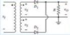
- AFrequency of the output voltage of full-wave rectifier is twice of frequency of its input voltage
- BFrequency of the output voltage of full-wave rectifier is one-half of frequency of its input voltage
- CFrequency of the output voltage of full-wave rectifier the same of frequency of its input voltage
63rectifier which results an output with a frequency twice input frequency that pulsates every half cycle of input voltage is
- Afull wave rectifier
- Bhalf wave rectifier
- Cmodulator
- Dregulator
64Refer to fig if D4 were to go short circuit, what would be the effect on the operation of the circuit?
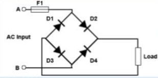
- AA decrease in the current through D1
- BA larger peak current through D2 and D3
- CFuse F1 would blow
- DA higher voltage across the load
65Zener diode are also known as
- AReverse bias diode
- BForward bias diode
- CNone of the mentioned
- DBreakdown diode
66The thinnest of all three regions is called the___________.
- AEmitter
- BCollector
- CBase
67Single phase full eave rectifier has the higher output voltage? Explain why?
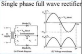
- AA bridge rectifier has a higher output voltage appears across the output points of the bridge.
- BThe full-wave rectifier has a higer outputs both half-cycles of the AC peakvoltage which averages to a lower voltage
- CThe same voltage in both cases
68One that clips positive part of voltage is known as
- Acurrent regulator
- Bclipper
- Cmultimeter
- Dvoltage regulator
69When referring to a junction field-effect transistor. Then describe the meaning of the threshhold voltage:
- AThe maximum gate-to-source voltage differential that is needed to create a conducting path between the source and drain terminals
- BThe minimum gate-to-source voltage differential that is needed to create a conducting path between the source and drain terminals
- COften called "pinch-off voltage" instead
70In figure shows, temperature modify the characteristics of a diode. What is the effect of temperature on reverse bias condition?
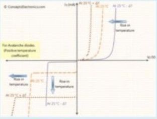
- AIn the reverse bias region increase in temperature causes the reverse saturation current of Si and Ge diodes doubles for every 10oC rise in temperature
- BIt increases forward voltage
- CIn the reverse bias region increase in temperature causes decrease in the cut-off voltage
71When component is the basic of a limiter circuit?
- ADiode
- BInductor
- CResistor
- DCapacitor
72When drain voltage equals the pinch-off-voltage, then drain current.............with the increase in drain voltage
- Aincreases
- Bnone of the above
- Cremains constant
- Ddecreases
73What type of clamper circuit is illustrated below
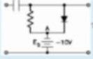
- APositive clamper with negative bias
- BNegative clamper with negative bias
- CNegative clamper with positive bias
- DPositive clamper with positive bias
74What type of diode circuit is used to add or restore a dc level to an electrical signal?
- Anone of the above
- BIC voltage regulator
- Cclipper or limiter
- Dclamper
75What characteristics of a diode makes it useful as an limiter?
- AIts ability to block current flow
- BIts acting like a short when forward biased and as open when reserved biased
- CIts being constructed from two dissimilar materials
- DIts barrier junction
76A half-wave rectifier circuit is represented in Figure. Identify N1 and N2
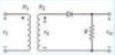
- AN1 and N2 are the positively charged vacancy in the forbidden band
- BN1 and N2 are the number of primary and secondary turns respectively
- CN1 and N2 are the positively charged vacancy in the conduction band
77Component in a clapping circuit which acts as a battery is
- Ainductor
- Btransformer
- Cresistor
- Dcapacitor
78What best describe the circuit?
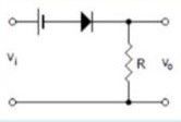
- AHalf-wave rectifier
- BFull-wave rectifier
- CClipper
- DClamper
79The purpose of the current limiting resistor in a zener circuit is to________
- Amaintain a constant current through the zener diode
- Bdrop the additional voltage from the power supply in order to maintain a constant voltage across the zener diode
- Cmaintain a constant current through the load resistor
80Under what condition depletion layer thickness is changed?
- Awhen a p-n junction is heavily doped
- Bwhen a p-n junction is lightly doped
- Cwhen an external voltage is applied to a p-n junction
Información
- Descripción
- Test sobre savethehell, creado por Mark Kim el 04/03/2020.
- Autor
- Mark Kim
- Idioma
- English
- Visitas
- 4
- Valoración
- Aún sin valoraciones Valora este test