Page 1
A Microprocessor -- also known as a CPU or central processing unit -- is a complete computation engine that is fabricated on a single chip.
The first microprocessor was the Intel 4004, introduced in 1971.The 4004 was not very powerful -- all it could do was add and subtract, and it could only do that 4 bits at a time.
Transistors is the number of transistors on the chip. You can see that the number of transistors on a single chip has risen steadily over the years. Microns is the width, in microns, of the smallest wire on the chip. For comparison, a human hair is 100 microns thick. As the feature size on the chip goes down, the number of transistors rises. Clock speed is the maximum rate that the chip can be clocked at. Clock speed will make more sense in the next section. Data Width is the width of the ALU. An 8-bit ALU can add/subtract/multiply/etc. two 8-bit numbers, while a 32-bit ALU can manipulate 32-bit numbers. An 8-bit ALU would have to execute four instructions to add two 32-bit numbers, while a 32-bit ALU can do it in one instruction. In many cases, the external data bus is the same width as the ALU, but not always. The 8088 had a 16-bit ALU and an 8-bit bus, while the modern Pentiums fetch data 64 bits at a time for their 32-bit ALUs. MIPS stands for "millions of instructions per second" and is a rough measure of the performance of a CPU. Modern CPUs can do so many different things that MIPS ratings lose a lot of their meaning, but you can get a general sense of the relative power of the CPUs from this column.
WHAT'S A CHIP? A chip is also called an integrated circuit. Generally it is a small, thin piece of silicon onto which the transistors making up the microprocessor have been etched. A chip might be as large as an inch on a side and can contain tens of millions of transistors. Simpler processors might consist of a few thousand transistors etched onto a chip just a few millimeters square.
Microprocessor Memory The previous section talked about the address and data buses, as well as the RD and WR lines. These buses and lines connect either to RAM or ROM -- generally both. In our sample microprocessor, we have an address bus 8 bits wide and a data bus 8 bits wide. That means that the microprocessor can address (28) 256 bytes of memory, and it can read or write 8 bits of the memory at a time. Let's assume that this simple microprocessor has 128 bytes of ROM starting at address 0 and 128 bytes of RAM starting at address 128.ROM stands for read-only memory. A ROM chip isprogrammed with a permanent collection of pre-set bytes. The address bus tells the ROM chip which byte to get and place on the data bus. When the RD line changes state, the ROM chip presents the selected byte onto the data bus.RAM stands for random-access memory. RAM contains bytes of information, and the microprocessor can read or write to those bytes depending on whether the RD or WR line is signaled. One problem with today's RAM chips is that they forget everything once the power goes off. That is why the computer needs ROM. RAM chip By the way, nearly all computers contain some amount of ROM (it is possible to create a simple computer that contains no RAM -- many microcontrollersdo this by placing a handful of RAM bytes on the processor chip itself -- but generally impossible to create one that contains no ROM). On a PC, the ROM is called the BIOS (Basic Input/Output System). When the microprocessor starts, it begins executing instructions it finds in the BIOS. The BIOS instructions do things like test the hardware in the machine, and then it goes to the hard disk to fetch the boot sector (see How Hard Disks Work for details). This boot sector is another small program, and the BIOS stores it in RAM after reading it off the disk. The microprocessor then begins executing the boot sector's instructions from RAM. The boot sector program will tell the microprocessor to fetch something else from the hard disk into RAM, which the microprocessor then executes, and so on. This is how the microprocessor loads and executes the entire operating system.
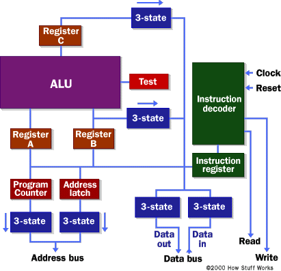
Microprocessor Logic To understand how a microprocessor works, it is helpful to look inside and learn about the logic used to create one. In the process you can also learn about assembly language -- the native language of a microprocessor -- and many of the things that engineers can do to boost the speed of a processor.A microprocessor executes a collection of machine instructions that tell the processor what to do. Based on the instructions, a microprocessor does three basic things: Using its ALU (Arithmetic/Logic Unit), a microprocessor can perform mathematical operations like addition, subtraction, multiplication and division. Modern microprocessors contain complete floating point processors that can perform extremely sophisticated operations on large floating point numbers. A microprocessor can move data from one memory location to another. A microprocessor can make decisions and jump to a new set of instructions based on those decisions. There may be very sophisticated things that a microprocessor does, but those are its three basic activities. The following diagram shows an extremely simple microprocessor capable of doing those three things: This is about as simple as a microprocessor gets. This microprocessor has: An address bus (that may be 8, 16 or 32 bits wide) that sends an address to memory A data bus (that may be 8, 16 or 32 bits wide) that can send data to memory or receive data from memory An RD (read) and WR (write) line to tell the memory whether it wants to set or get the addressed location A clock line that lets a clock pulse sequence the processor A reset line that resets the program counter to zero (or whatever) and restarts execution Let's assume that both the address and data buses are 8 bits wide in this example.Here are the components of this simple microprocessor: Registers A, B and C are simply latches made out of flip-flops. (See the section on "edge-triggered latches" in How Boolean Logic Works for details.) The address latch is just like registers A, B and C. The program counter is a latch with the extra ability to increment by 1 when told to do so, and also to reset to zero when told to do so. The ALU could be as simple as an 8-bit adder (see the section on adders in How Boolean Logic Worksfor details), or it might be able to add, subtract, multiply and divide 8-bit values. Let's assume the latter here. The test register is a special latch that can hold values from comparisons performed in the ALU. An ALU can normally compare two numbers and determine if they are equal, if one is greater than the other, etc. The test register can also normally hold a carry bit from the last stage of the adder. It stores these values in flip-flops and then the instruction decoder can use the values to make decisions. There are six boxes marked "3-State" in the diagram. These are tri-state buffers. A tri-state buffer can pass a 1, a 0 or it can essentially disconnect its output (imagine a switch that totally disconnects the output line from the wire that the output is heading toward). A tri-state buffer allows multiple outputs to connect to a wire, but only one of them to actually drive a 1 or a 0 onto the line. The instruction register and instruction decoder are responsible for controlling all of the other components. Although they are not shown in this diagram, there would be control lines from the instruction decoder that would: Tell the A register to latch the value currently on the data bus Tell the B register to latch the value currently on the data bus Tell the C register to latch the value currently output by the ALU Tell the program counter register to latch the value currently on the data bus Tell the address register to latch the value currently on the data bus Tell the instruction register to latch the value currently on the data bus Tell the program counter to increment Tell the program counter to reset to zero Activate any of the six tri-state buffers (six separate lines) Tell the ALU what operation to perform Tell the test register to latch the ALU's test bits Activate the RD line Activate the WR line Coming into the instruction decoder are the bits from the test register and the clock line, as well as the bits from the instruction register.
Microprocessor Instructions Even the incredibly simple microprocessor shown in the previous example will have a fairly large set of instructions that it can perform. The collection of instructions is implemented as bit patterns, each one of which has a different meaning when loaded into the instruction register. Humans are not particularly good at remembering bit patterns, so a set of short words are defined to represent the different bit patterns. This collection of words is called the assembly language of the processor. An assembler can translate the words into their bit patterns very easily, and then the output of the assembler is placed in memory for the microprocessor to execute.Here's the set of assembly language instructions that the designer might create for the simple microprocessor in our example: LOADA mem - Load register A from memory address LOADB mem - Load register B from memory address CONB con - Load a constant value into register B SAVEB mem - Save register B to memory address SAVEC mem - Save register C to memory address ADD - Add A and B and store the result in C SUB - Subtract A and B and store the result in C MUL - Multiply A and B and store the result in C DIV - Divide A and B and store the result in C COM - Compare A and B and store the result in test JUMP addr - Jump to an address JEQ addr - Jump, if equal, to address JNEQ addr - Jump, if not equal, to address JG addr - Jump, if greater than, to address JGE addr - Jump, if greater than or equal, to address JL addr - Jump, if less than, to address JLE addr - Jump, if less than or equal, to address STOP - Stop execution If you have read How C Programming Works, then you know that this simple piece of C code will calculate the factorial of 5 (where the factorial of 5 = 5! = 5 * 4 * 3 * 2 * 1 = 120): a=1;f=1;while (a At the end of the program's execution, the variable f contains the factorial of 5. Assembly Language A C compiler translates this C code into assembly language. Assuming that RAM starts at address 128 in this processor, and ROM (which contains the assembly language program) starts at address 0, then for our simple microprocessor the assembly language might look like this: // Assume a is at address 128// Assume F is at address 1290 CONB 1 // a=1;1 SAVEB 1282 CONB 1 // f=1;3 SAVEB 1294 LOADA 128 // if a > 5 the jump to 175 CONB 56 COM7 JG 178 LOADA 129 // f=f*a;9 LOADB 12810 MUL11 SAVEC 12912 LOADA 128 // a=a+1;13 CONB 114 ADD15 SAVEC 12816 JUMP 4 // loop back to if17 STOP ROM So now the question is, "How do all of these instructions look in ROM?" Each of these assembly language instructions must be represented by a binary number. For the sake of simplicity, let's assume each assembly language instruction is given a unique number, like this: LOADA - 1 LOADB - 2 CONB - 3 SAVEB - 4 SAVEC mem - 5 ADD - 6 SUB - 7 MUL - 8 DIV - 9 COM - 10 JUMP addr - 11 JEQ addr - 12 JNEQ addr - 13 JG addr - 14 JGE addr - 15 JL addr - 16 JLE addr - 17 STOP - 18 The numbers are known as opcodes. In ROM, our little program would look like this: // Assume a is at address 128// Assume F is at address 129Addr opcode/value0 3 // CONB 11 12 4 // SAVEB 1283 1284 3 // CONB 15 16 4 // SAVEB 1297 1298 1 // LOADA 1289 12810 3 // CONB 511 512 10 // COM13 14 // JG 1714 3115 1 // LOADA 12916 12917 2 // LOADB 12818 12819 8 // MUL20 5 // SAVEC 12921 12922 1 // LOADA 12823 12824 3 // CONB 125 126 6 // ADD27 5 // SAVEC 12828 12829 11 // JUMP 430 831 18 // STOP You can see that seven lines of C code became 18 lines of assembly language, and that became 32 bytes in ROM. Decoding The instruction decoder needs to turn each of the opcodes into a set of signals that drive the different components inside the microprocessor. Let's take the ADD instruction as an example and look at what it needs to do: During the first clock cycle, we need to actually load the instruction. Therefore the instruction decoder needs to: activate the tri-state buffer for the program counter activate the RD line activate the data-in tri-state buffer latch the instruction into the instruction register During the second clock cycle, the ADD instruction is decoded. It needs to do very little: set the operation of the ALU to addition latch the output of the ALU into the C register During the third clock cycle, the program counter is incremented (in theory this could be overlapped into the second clock cycle). Every instruction can be broken down as a set of sequenced operations like these that manipulate the components of the microprocessor in the proper order. Some instructions, like this ADD instruction, might take two or three clock cycles. Others might take five or six clock cycles.
New Page
New Page
New Page
New Page
Want to create your own Notes for free with GoConqr? Learn more.