
Mapa mental
Semi Conductor Junctions
Conteúdo do mapa
Semi Conductor Junctions
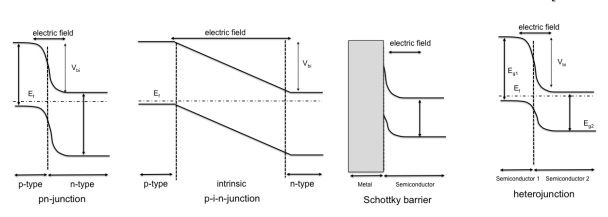
4 Main types
- PN
- PIN
- Schottky barrier
- Heterojunction
Basic operation
- each semiconductor = built in potential
- junctions generate a strong electric field
- between two semi conductors (N-Type) and (P-type)
- n-type electrons near interface cross to p-type
- leaves a positively charged area
- leaves a positively charged area
- P-type hole cross to n-type side
- leaves a negatively charged area
- Creates a potential barrier, with no mobile charges
- prevents flow of electrons of holes through potential barrier
- An electric field drives electrons and holes in opposite directions
- prevents flow of electrons of holes through potential barrier
- Creates a potential barrier, with no mobile charges
- leaves a negatively charged area
- n-type electrons near interface cross to p-type
- between two semi conductors (N-Type) and (P-type)
- junctions generate a strong electric field
- each semiconductor = built in potential
formation of electron/hole pair via light absorbtion = fundamental to solar cell operation
- Excitation from valence band to conduction band = fundamental absorption
- total energy and momentum must be conserved
- absorption in GaAs and Si = determined by electron band strucutres
- Periodic array produces varying band structures
- GaAs = direct band gap semiconductor
- photon energy > Eg can excited from VB to CB in a relatively efficient manner
- Si = indirect band gap semiconductor
- complicated absorption process
- phonons are involved in the conversion of a photo to electron-hole pairs
- momentum conservation
- complicated process reduces the absorption efficicney of light by a semiconductor - SI < efficient < GaAs
- phonons are involved in the conversion of a photo to electron-hole pairs
- complicated absorption process
- GaAs = direct band gap semiconductor
- Periodic array produces varying band structures
- absorption in GaAs and Si = determined by electron band strucutres
- total energy and momentum must be conserved
- Excitation from valence band to conduction band = fundamental absorption
Dye Sensitised Solar Cell
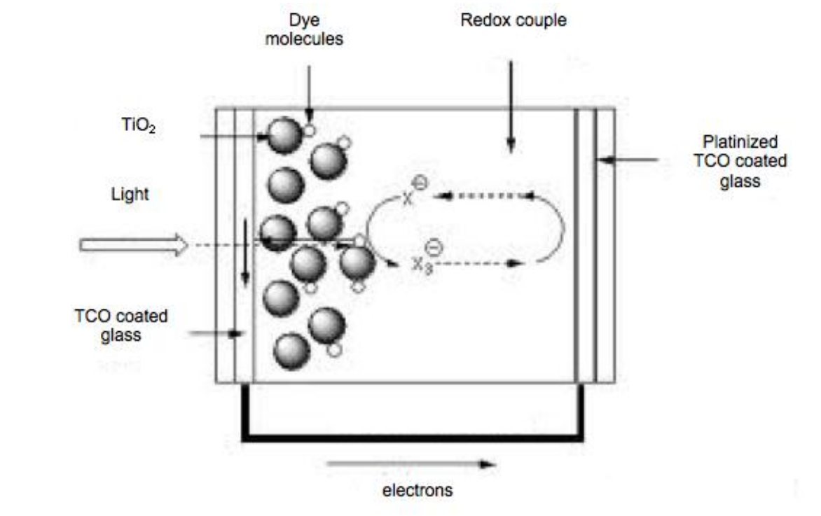
- layer of TiO2 particles
- covered in a sensitive dye that absorbs sunlight
- TiO2 is immersed in an electrolyte solution
- light passes through the transparent electrode into the dye layer where it can excite electrons
- electrons flow into TiO2 and flow towards the anode
- collected here, used to power a load i.e. a light
- after flowing through the external circuit, reintroduced into electrolyte by the cathode
- electrolyte transports the electrons back to the dye molecules
- after flowing through the external circuit, reintroduced into electrolyte by the cathode
- collected here, used to power a load i.e. a light
- electrons flow into TiO2 and flow towards the anode
- light passes through the transparent electrode into the dye layer where it can excite electrons
- TiO2 is immersed in an electrolyte solution
- covered in a sensitive dye that absorbs sunlight
- layer of TiO2 particles
Imagens e arquivos do mapa
Informações
- Descrição
- Mapa Mental sobre Semi Conductor Junctions, criado por Tom Piggott em 25-05-2017.
- Criado por
- Tom Piggott
- Visualizações
- 1
- Avaliação