
Karteikarten
PCB design
Karten in diesem Stapel (22)
- 1What is PCB used for? What is it usually made of (two things)?Printed circuit boards are used to hold and connect the electronic components of a device. It is usually made of copper and some sort of non-conductive coating.
- 2What layers cannot me used to mount surface-mount components in a four-layer PCB? Top? 2nd layer? 3rd layer? Bottom? And why?You cannot mount surface-mount components on the second and third layers, since these are covered by the bottom/top layer.
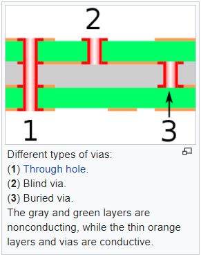
- 3What is via used for in PCB? What are the three different kinds of vias and describe their differences in construction.A via is a hole between the layers of a PCB that lets the electric signal move between layers. A blind via is only visible on one side of the PCB, a buried via connects internal layers and is not visible on the surface, and a thermal via is used to lead heat away from certain components on the board.
- 4Draw a via, show out what is the via ring thickness and what is the via hole diameter.

- 5What are meanings of clearance and minimal trace width setting in PCB design? And why are they needed?Clearance is the shortest allowed distance through air between two conductors. The distance cannot be too small, since environmental factors like humidity and dust can increase the risk of shorts between conductors.
Minimal trace width decides how thin the copper routes between components can be. A PCB that handles high voltages will need a wider trace. - 6What are the PCB design differences for mounting of surface-mount components and through-hole-mount components? Which one is more popular in PCB design now?Surface-mount components are more common now, since they take up less space than the through-hole-mount components.
- 7What is solder mask in PCB production and assembly? And what is it used for?The solder mask is the covering that is usually green. It is used to protect the copper and only keep the solder pads exposed. This way the copper is protected from the element and solder doesn’t go in places where it shouldn’t.
- 8What is silkscreen in PCB production and assembly? And what is it used for?The silkscreen is the white text on the circuit board that marks out where components go (to make sure they’re not attached upside down) and what they are called. If this gets on a solder pad, the solder joint will be much weaker.
- 9What is paste mask in PCB production and assembly? And what is it used for?The solder mask is used to produce a soldering stencil. It shows the areas where solder paste needs to be applied to attach surface-mount components.
- 10What is board outline in PCB production and assembly? And what is it used for?The board outline defines the shape and size of the PCB. Seeing this makes it easier to place the components in a way that makes sense.
- 11What is ground flooding in PCB design? And what is it used for?Ground flooding is when you fill an unused area of the PCB with copper. That area is then used as a ground point so that a ground is easily accessible to all components.
- 12What are the plated drill and non-plated drill? And what is the difference between them?A plated drill has a thin layer of copper lining the walls of the hole. This gives better mechanical stability. A non-plated drill has no copper on the walls, so they have no electrical properties. These are easier to manufacture but not as functional for multi-layer PCBs.
- 13Is it ok for silkscreen to overlap mounting pads in PCB design? And why?No. If silkscreen overlaps the mounting pads the ink will prevent the solder from flowing correctly and will result in a much weaker solder point.
- 14What is used to connect and mount terminals of components to their mounting pads on PCB? And briefly describe how it is used to do so.Components are attached to the mounting pads by soldering. This can be done by for example applying solder paste using a stencil and then placing the components on the paste. You can also solder by hand using a soldering iron.
- 15Why are power supply and grounding traces in PCB design usually wider than signal traces?A long and narrow trace has a higher resistance compared to the short and wide traces. A thin trace going to or from a power supply can be damaged by too high currents.
- 16For high-speed signal trace routing, people typically want the trace to be routed thin, short and close to the ground, which three factors are the in the consideration? And why?In high-speed signal trace routing the traces might require a specific length and width to control impedance and minimize reflections and inductive coupling.
- 17Why different grounds are recommended to be mostly separated and only be joined at the final power supply ground point? What are in the consideration?To avoid noisy components affecting other components.
- 18Are there all values available to buy for the passive components on the market? And why?There are many different values available, but not every single one. Capacitances have a wider range of values available compared to resistors.
- 19What are the meanings of ideal and non-ideal passive components?An ideal passive component does exactly what we want it to do, and a non-ideal one is how components are in real life. A real resistor might not have the exact same resistance as it says on the packaging.
- 20Can a 10Ω and a 1M Ω resistors have the same small component size of 0402? And can a 10pF and a 100µF capacitor have the same small component size of 0402? And why?Yes, because they can both be made from different materials. A smaller resistor or capacitor may use different dielectrics to achieve different values all while keeping the same measurements.
- 21Why resistor has the power range rating? Why capacitor has the voltage range rating? How would they fail if you use them above these ratings? (describe their failure mode)A resistor’s power rating is the amount of heat it can dissipate without affecting its performance. If this is exceeded the resistor will melt or catch fire.
A capacitor’s voltage rating is the amount of voltage that the capacitor can safely store and be exposed to safely. If this is exceeded the capacitor could explode. - 22What is the meaning of tolerance rating for the passive components? How high the percentage can the tolerance ratings of commercial resistor and capacitor be in market?The tolerance rating is how much a component is allowed to vary from its value. For capacitors the rating can be up to 80%. For resistors the tolerance can be up to 20%
Informationen
- Beschreibung
- Karteikarten am PCB design, erstellt von Emma Alamaa am 08/03/2021.
- Erstellt von
- Emma Alamaa
- Aufrufe
- 6
- Bewertung