
Mindmap
Chapter 11: Boolean Algebra (2621)

Inhalt der Mindmap
Chapter 11: Boolean Algebra (2621)
11.1 BOOLEAN ALGEBRA
- Boolean algebra turns out to be a convenient tool in two areas:
- ■ Analysis: It is an economical way of describing the function of digital circuitry.
- ■ Design: Given a desired function, Boolean algebra can be applied to develop a simplified implementation of that function.
- Thus, a variable may take on the value 1 (TRUE) or 0 (FALSE).
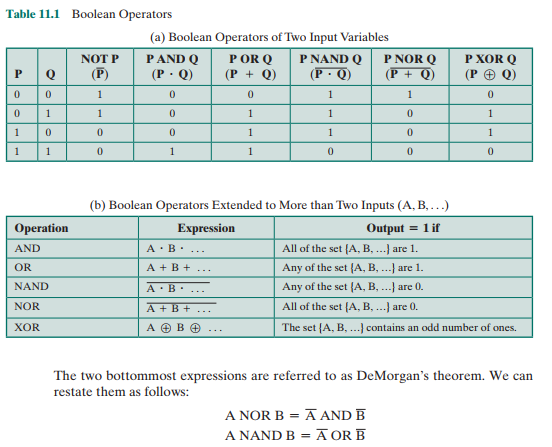
- A AND B = A . B A OR B = A + B NOT A = A bar
- n the absence of parentheses, the AND operation takes precedence over the OR operation.
- Table 11.1a defines the basic logical operations in a form known as a truth table, which lists the value of an operation for every possible combination of values of operands
- XOR, NAND, and NOR. The exclusive-or (XOR) of two logical operands is 1 if and only if exactly one of the operands has the value 1
- NAND function is the complement (NOT) of the AND function, and the NOR is the complement of OR:
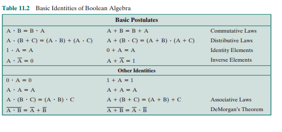
- There are two classes of identities: basic rules (or postulates), which are stated without proof, and other identities that can be derived from the basic postulates
- One of the two distributive laws is worth noting because it differs from what we would find in ordinary algebra: A + (B # C) = (A + B) . (A + C)
- Boolean algebra turns out to be a convenient tool in two areas:
11.2 GATES
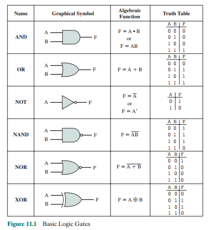
- The basic gates used in digital logic are AND, OR, NOT, NAND, NOR, and XOR.
- Each gate is defined in three ways: graphic symbol, algebraic notation, and truth table
- Note that the inversion (NOT) operation is indicated by a circle.
- all of the gates except NOT can have more than two inputs
- When one or more of the values at the input are changed, the correct output signal appears almost instantaneously, delayed only by the propagation time of signals through the gate (known as the gate delay).
- we say that to assert a signal is to cause a signal line to make a transition from its logically false (0) state to its logically true (1) state. The true (1) state is either a high or low voltage state, depending on the type of electronic circuitry.
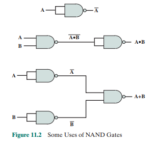
- Design and fabrication are simpler if only one or two types of gates are used.
- The following are functionally complete sets: ■ AND, OR, NOT ■ AND, NOT ■ OR, NOT ■ NAND ■ NOR
- For the AND and NOT gates to form a functionally complete set, there must be a way to synthesize the OR operation from the AND and NOT operations. This can be done by applying DeMorgan’s theorem:
- OR and NOT operations are functionally complete because they can be used to synthesize the AND operation
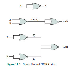
- Figure 11.2 shows how the AND, OR, and NOT functions can be implemented solely with NAND gates, and Figure 11.3 shows the same thing for NOR gates.
11.3 COMBINATIONAL CIRCUITS
- A combinational circuit is an interconnected set of gates whose output at any time is a function only of the input at that time
- a combinational circuit consists of n binary inputs and m binary outputs. As with a gate, a combinational circuit can be defined in three ways:
- ■ Truth table: For each of the 2n possible combinations of input signals, the binary value of each of the m output signals is listed.
- ■ Graphical symbols: The interconnected layout of gates is depicted.
- ■ Boolean equations: Each output signal is expressed as a Boolean function of its input signals
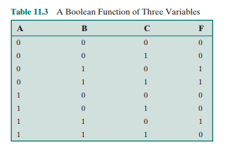
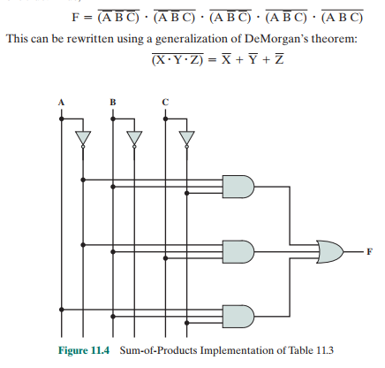
- We can express this function by simply itemizing the combinations of values of A, B, and C that cause F to be 1:
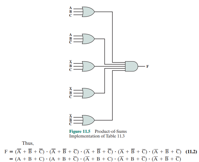
- We can also say that the output is 1 if none of the input combinations that produce 0 is true.
- This is in the product of sums (POS) form. For clarity, NOT gates are not shown. Rather, it is assumed that each input signal and its complement are available.
- Boolean function can be realized in either SOP or POS form
- the choice would depend on whether the truth table contains more 1s or 0s for the output function: The SOP has one term for each 1, and the POS has one term for each 0. However, there are other considerations:
- ■ It is often possible to derive a simpler Boolean expression from the truth table than either SOP or POS.
- with a simpler Boolean expression, fewer gates will be needed to implement the function. Three methods that can be used to achieve simplification are
- ■ Algebraic simplification
- application of the identities of Table 11.2 to reduce the Boolean expression to one with fewer elements.
- an equivalent expression is
- application of the identities of Table 11.2 to reduce the Boolean expression to one with fewer elements.
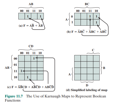
- ■ Karnaugh maps
- representing a Boolean function of a small number (up to four) of variables.
- The map is an array of 2n squares, representing all possible combinations of values of n binary variables
- list the combinations in the order 00, 01, 11, 10
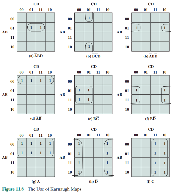
- Any two squares that are adjacent differ in only one of the variables. If two adjacent squares both have an entry of one, then the corresponding product terms differ in only one variable. In such a case, the two terms can be merged by eliminating that variable. For example, in Figure 11.8a, the two adjacent squares correspond to the two terms ABCD and ABCD. Thus, the function expressed is
- This process can be extended in several ways. First, the concept of adjacency can be extended to include wrapping around the edge of the map. Thus, the top square of a column is adjacent to the bottom square, and the leftmost square of a row is adjacent to the rightmost square
- Second, we can group not just 2 squares but 2n adjacent squares (i.e., 2, 4, 8, etc.)
- We can summarize the rules for simplification as follows:
- 1. Among the marked squares (squares with a 1), find those that belong to a unique largest block of 1, 2, 4, or 8 and circle those blocks.
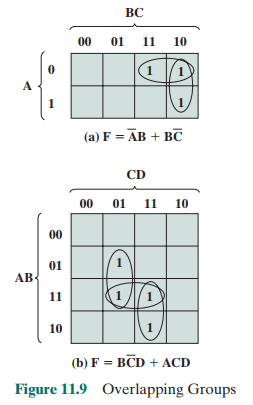
- 2. Select additional blocks of marked squares that are as large as possible and as few in number as possible, but include every marked square at least once. The results may not be unique in some cases. For example, if a marked square combines with exactly two other squares, and there is no fourth marked square to complete a larger group, then there is a choice to be made as to which of the two groupings to choose. When you are circling groups, you are allowed to use the same 1 value more than once
- 3. Continue to draw loops around single marked squares, or pairs of adjacent marked squares, or groups of four, eight, and so on in such a way that every marked square belongs to at least one loop; then use as few of these blocks as possible to include all marked squares.
- Figure 11.9a, based on Table 11.3
- Finally, before going from the map to a simplified Boolean expression, any group of 1s that is completely overlapped by other groups can be eliminated.
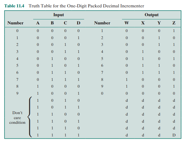
- We would like to develop the Boolean expressions for a circuit that adds 1 to a packed decimal digit. For packed decimal, each decimal digit is represented by a 4-bit code, in the obvious way. Thus, 0 = 0000, 1 = 0001, c, 8 = 1000, and 9 = 1001. The remaining 4-bit values, from 1010 to 1111, are not used. This code is also referred to as Binary Coded Decimal (BCD)
- Table 11.4 shows the truth table for producing a 4-bit result that is one more than a 4-bit BCD input. The addition is modulo 10. Thus, 9 + 1 = 0. Also, note that six of the input codes produce “don’t care” results, because those are not valid BCD inputs. Figure 11.10 shows the resulting Karnaugh maps for each of the output variables. The d squares are used to achieve the best possible groupings.
- representing a Boolean function of a small number (up to four) of variables.
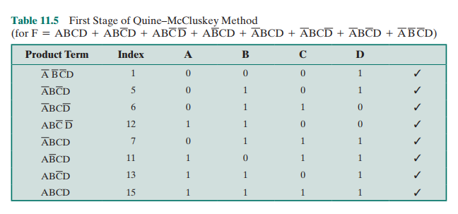
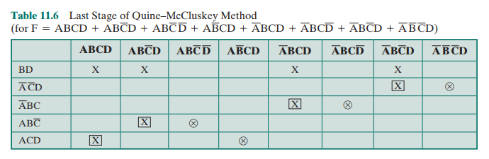
- ■ Quine–McCluskey tables
- For more than four variables, the Karnaugh map method becomes increasingly cumbersome.
- In cases in which some columns have neither a circle nor a square, additional processing is required.
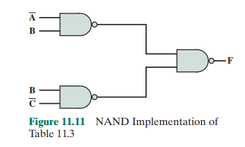
- nand and nor implementations
- Another consideration in the implementation of Boolean functions concerns the types of gates used.
- Multiplexers
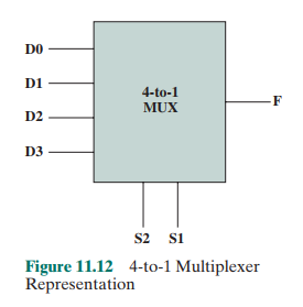
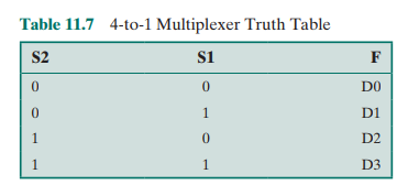
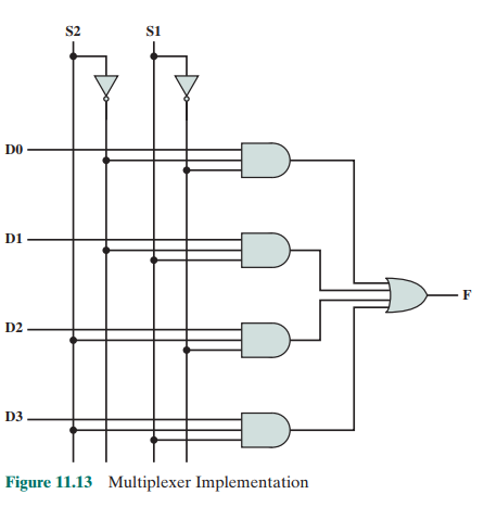
- The multiplexer connects multiple inputs to a single output.
- There are four input lines, labeled D0, D1, D2, and D3. One of these lines is selected to provide the output signal F
- To select one of the four possible inputs, a 2-bit selection code is needed, and this is implemented as two select lines labeled S1 and S2.
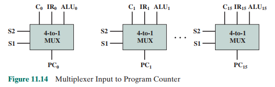
- Multiplexers are used in digital circuits to control signal and data routing. An example is the loading of the program counter (PC)
- The value to be loaded into the program counter may come from one of several different sources:
- ■ A binary counter, if the PC is to be incremented for the next instruction. ■ The instruction register, if a branch instruction using a direct address has just been executed. ■ The output of the ALU, if the branch instruction specifies the address using a displacement mode.
- These various inputs could be connected to the input lines of a multiplexer, with the PC connected to the output line. The select lines determine which value is loaded into the PC. Because the PC contains multiple bits, multiple multiplexers are used, one per bit. Figure 11.14 illustrates this for 16-bit addresses.
- Decoders
- A decoder is a combinational circuit with a number of output lines, only one of which is asserted at any time.
- In general, a decoder has n inputs and 2n outputs. Figure 11.15 shows a decoder with three inputs and eight outputs.
- Decoders find many uses in digital computers. One example is address decoding.
- With an additional input line, a decoder can be used as a demultiplexer. The demultiplexer performs the inverse function of a multiplexer; it connects a single input to one of several outputs.
- Read-Only Memory
- Combinational circuits are often referred to as “memoryless” circuits, because their output depends only on their current input and no history of prior inputs is retained.
- there is one sort of memory that is implemented with combinational circuits, namely read-only memory (ROM).
- ROM is a memory unit that performs only the read operation. This implies that the binary information stored in a ROM is permanent and was created during the fabrication process
- a given input to the ROM (address lines) always produces the same output (data lines)
- the outputs are a function only of the present inputs, the ROM is in fact a combinational circuit
- A ROM can be implemented with a decoder and a set of OR gates.
- Adders
- So far, we have seen how interconnected gates can be used to implement such functions as the routing of signals, decoding, and ROM
- essential area not yet addressed is that of arithmetic
- Binary addition differs from Boolean algebra in that the result includes a carry term
- ■ Algebraic simplification
- with a simpler Boolean expression, fewer gates will be needed to implement the function. Three methods that can be used to achieve simplification are
- ■ It may be preferable to implement the function with a single gate type (NAND or NOR).
- ■ It is often possible to derive a simpler Boolean expression from the truth table than either SOP or POS.
- the choice would depend on whether the truth table contains more 1s or 0s for the output function: The SOP has one term for each 1, and the POS has one term for each 0. However, there are other considerations:
11.4 SEQUENTIAL CIRCUITS
- Combinational circuits implement the essential functions of a digital computer
- except for the special case of ROM, they provide no memory or state information, elements also essential to the operation of a digital computer
- latter purposes, a more complex form of digital logic circuit is used: the sequential circuit.
- current output of a sequential circuit depends not only on the current input, but also on the past history of inputs
- the current output of a sequential circuit depends on the current input and the current state of that circuit.
- As will be seen, the sequential circuit makes use of combinational circuits
- Flip-Flops
- which share two properties:
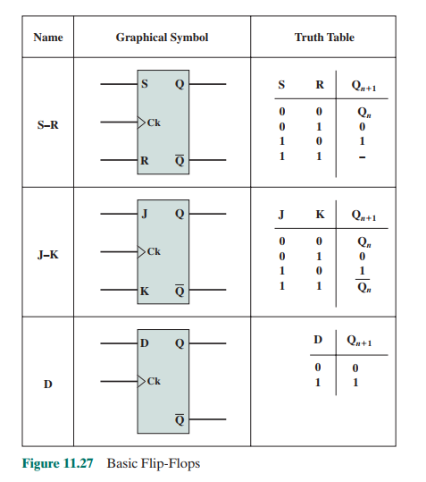
- ■ The flip-flop is a bistable device. It exists in one of two states and, in the absence of input, remains in that state. Thus, the flip-flop can function as a 1-bit memory. ■ The flip-flop has two outputs, which are always the complements of each other. These are generally labeled Q and Q.
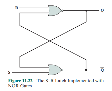
- the s–r latch
- known as the S–R flipflop
- The circuit has two inputs, S (Set) and R (Reset)
- and two outputs, Q and Q, and consists of two NOR gates connected in a feedback arrangement.
- The S–R latch can be defined with a table similar to a truth table, called a characteristic table
- clocked s–r flip-flop
- The output of the S–R latch changes, after a brief time delay, in response to a change in the input. This is referred to as asynchronous operation
- events in the digital computer are synchronized to a clock pulse, so that changes occur only when a clock pulse occurs.
- d flip-flop
- j–k flip-flop
- which share two properties:
- Registers
- As we know, a register is a digital circuit used within the CPU to store one or more bits of data. Two basic types of registers are commonly used: parallel registers and shift registers.
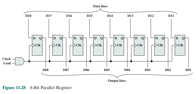
- parallel registers
- a set of 1-bit memories that can be read or written simultaneously. It is used to store data
- The 8-bit register of Figure 11.28 illustrates the operation of a parallel register using D flip-flops. A control signal, labeled load, controls writing into the register from signal lines, D11 through D18. These lines might be the output of multiplexers, so that data from a variety of sources can be loaded into the register.
- shift register
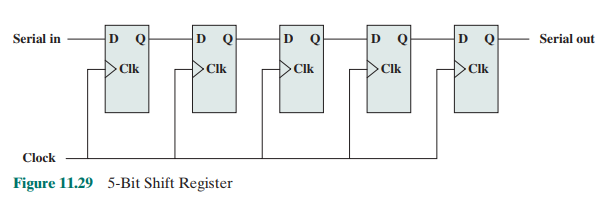
- A shift register accepts and/or transfers information serially
- Figure 11.29, which shows a 5-bit shift register constructed from clocked D flip-flops. Data are input only to the leftmost flip-flop. With each clock pulse, data are shifted to the right one position, and the rightmost bit is transferred out.
- Shift registers can be used to interface to serial I/O devices. In addition, they can be used within the ALU to perform logical shift and rotate functions
- In the latter capacity, they need to be equipped with parallel read/write circuitry as well as serial.
- Counters
- Another useful category of sequential circuit is the counter
- A counter is a register whose value is easily incremented by 1 modulo the capacity of the register; that is, after the maximum value is achieved the next increment sets the counter value to 0. Thus, a register made up of n flip-flops can count up to 2n - 1.
- Counters can be designated as asynchronous or synchronous
- Asynchronous counters are relatively slow because the output of one flip-flop triggers a change in the status of the next flip-flop
- synchronous counter, all of the flip-flops change state at the same time. Because the latter type is much faster, it is the kind used in CPUs.
- Asynchronous
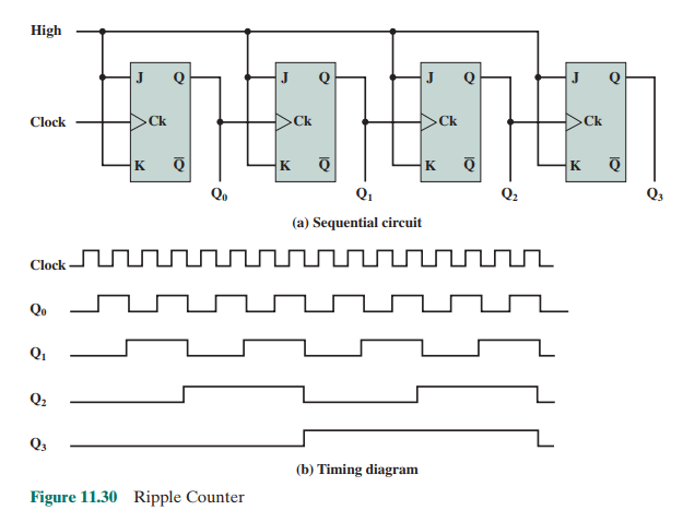
- ripple counter
- asynchronous counter is also referred to as a ripple counter, because the change that occurs to increment the counter starts at one end and “ripples” through to the other end.
- ripple counter
- Synchronous
- synchronous counters
- The ripple counter has the disadvantage of the delay involved in changing value, which is proportional to the length of the counter.
- synchronous counters
11.5 PROGRAMMABLE LOGIC DEVICES
- Programmable Logic Array
- The PLA is based on the fact that any Boolean function (truth table) can be expressed in a sum-of-products (SOP) form
- PLA consists of a regular arrangement of NOT, AND, and OR gates on a chip
- Field-Programmable Gate Array
- Programmable Logic Array
Bilder und Dateien der Mindmap





Informationen
- Beschreibung
- Computer Science Mindmap am Chapter 11: Boolean Algebra (2621), erstellt von Gideon Van am 25/07/2019.
- Erstellt von
- Gideon Van · Jul 2019
- Aktualisiert
- 28 Jul 2019
- Aufrufe
- 1
- Bewertung