
Diagrama de flujo
Sin título
Contenido del diagrama
SEQUENTIAL CIRCUITS
Combinational circuits implement the essential functions of a digital computer.
For the latter purposes, a more complex form of digital logic circuit is used: the sequential circuit.
we will examine some simple but useful examples of sequential circuits. As will be seen, the sequential circuit makes use of combinational circuits.
Flip-Flops
The simplest form of sequential circuit is the flip-flop. There are a variety of flipflops, all of which share two properties:
The flip-flop is a bistable device. It exists in one of two states and, in the a bsence of input, remains in that state. Thus, the flip-flop can function as a 1-bit memory.
The flip-flop has two outputs, which are always the complements of each other.
THE S–R LATCH
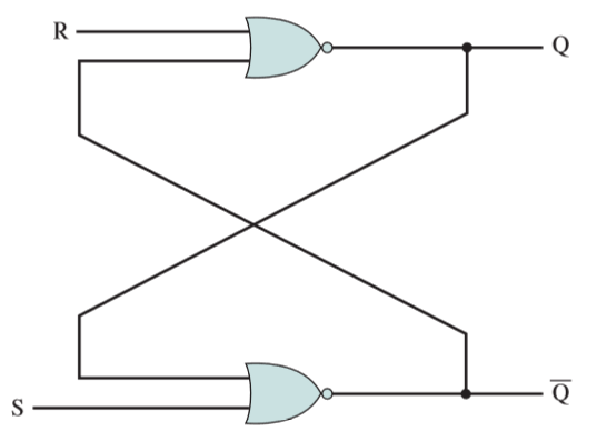
The next figure shows a common configuration known as the S–R flip-flop or S–R latch. The circuit has two inputs, S (Set) and R (Reset), and two outputs, Q and Q, and consists of two NOR gates connected in a feedback arrangement.
THE S–R LATCH
The next figure shows a common configuration known as the S–R flip-flop or S–R latch. The circuit has two inputs, S (Set) and R (Reset), and two outputs, Q and Q, and consists of two NOR gates connected in a feedback arrangement.
CLOCKED S–R FLIP-FLOP The output of the S–R latch changes, after a brief time delay, in response to a change in the input. This is referred to as asynchronous operation. More typically, events in the digital computer are synchronized to a clock pulse, so that changes occur only when a clock pulse occurs.
D FLIP-FLOP One problem with S–R flip-flop is that the condition R = 1, S = 1 must be avoided. One way to do this is to allow just a single input. The D flip-flop accomplishes this.
J–K FLIP-FLOP Another useful flip-flop is the J–K flip-flop. Like the S–R flip-flop, it has two inputs. However, in this case all possible combinations of input values are valid.
Registers
As an example of the use of flip-flops, let us first examine one of the essential elements of the CPU: the register. As we know, a register is a digital circuit used within the CPU to store one or more bits of data. Two basic types of registers are commonly used: parallel registers and shift registers.
PARALLEL REGISTERS A parallel register consists of a set of 1-bit memories that can be read or written simultaneously. It is used to store data. The registers that we have discussed throughout this book are parallel registers.
SHIFT REGISTER A shift register accepts and/or transfers information serially. Shift registers can be used to interface to serial I/O devices. In addition, they can be used within the ALU to perform logical shift and rotate functions.
PROGRAMMABLE LOGIC DEVICES
As the level of integration provided by integrated circuits increases, other considerations apply. Early integrated circuits, using small-scale integration (SSI), provided from one to ten gates on a chip. Each gate is treated independently, in the building-block approach described so far. To construct a logic function, a number of these chips are laid out on a printed circuit board and the appropriate pin interconnections are made.
Programmable Logic Array The PLA is based on the fact that any Boolean function (truth table) can be expressed in a sum-of-products (SOP) form, as we have seen. The PLA consists of a regular arrangement of NOT, AND, and OR gates on a chip.
Each chip input is passed through a NOT gate so that each input and its complement are available to each AND gate. The output of each AND gate is available to each OR gate, and the output of each OR gate is a chip output. By making the appropriate connections, arbitrary SOP expressions can be implemented.
Field-Programmable Gate Array An FPGA consists of an array of uncommitted circuit elements, called logic blocks, and interconnect resources.
The key components of an FPGA are:
Logic block: The configurable logic blocks are where the computation of the user’s circuit takes place.
I/O block: The I/O blocks connect I/O pins to the circuitry on the chip.
Interconnect: These are signal paths available for establishing connections among I/O blocks and logic blocks.
TEC,Sede central,Fundamentos de organizacion de computadores
Escuela de ingenieria en computacion
Resumen #4(W.Stallings, cap. 11 - Lógica Digital) PARTE 2
Jossy Mejia Vargas 2017109693
Miercoles 30 de agosto del 2017, 2 semestre, Esteban Arias Mendez
Información
- Descripción
- Diagrama sobre Sin título, creado por Jossy Ivan Mejia Vargas el 04/09/2017.
- Creado por
- Jossy Ivan Mejia Vargas · sep 2017
- Actualizado
- 5 sep 2017
- Visitas
- 0
- Valoración