325500
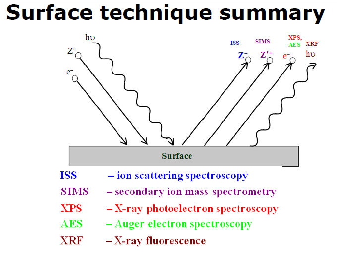
SURFACE ANALYSIS
Nota:
- use all the techniques to characterize the atoms of the surface
- INTRO
- WHY?
- 1. Coatings
Nota:
- want to see how the surface looks like
- 2. CIP process
(adsorption/ desorption)
Nota:
- carbon import process wan to see how porous the surface is - microscopically, the surface is not a straight line (more porous - more reactive)
- 3. corrosion
- 4. friction
- 5. heterogeneous catalysis
- 6. Environmental applications -->
wastewater/gas treatments
Nota:
- high porosity absorbs more pollutant (e.g. water tap)
- 1. Coatings
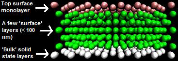
- BASIC CONCEPTS
- Discriminate for the (small amount) of
‘surface’ against the (large amount) of
the ‘bulk’
- 'Surface’ --> direct contact
(interface) with other
phases, e.g. gas or liquid.
- why is it important to analyse surface?
Nota:
- in Carbon Import Process (CIP) - need to analyse activity carbon - to absorb gold complex from ores. analyse the surface of the activity carbon to see the changes before & after the process of absorbing the complex (porous?)
- describe the concept
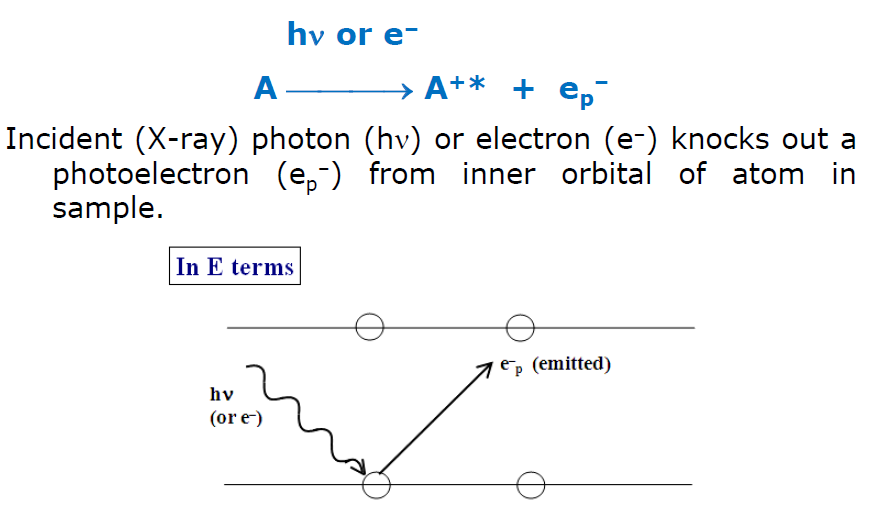
Nota:
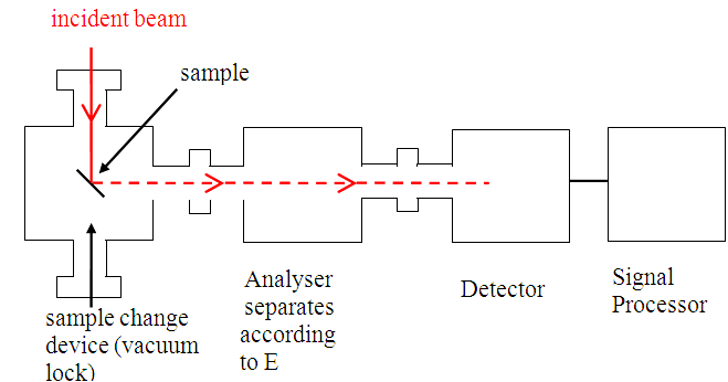
- Fire a particle from a source (can be a thermionic gun) - heat up the source. - emits particles (e.g. electrons/ions etc) - travel through a path of vaccum (no obstruction) - hit the surface of the sample (results in emission of some of the electron from the surface) (some particles bounce back) - measure the emitted particles/energy
- Discriminate for the (small amount) of
‘surface’ against the (large amount) of
the ‘bulk’
- What is a surface?
- Depends on the technique
(& does not usually mean
only the first layer of atoms)
- 0.1 nm (AES; STM) --> 100 nm (XRD)
- Depends on the technique
(& does not usually mean
only the first layer of atoms)
- In situ vs. ex situ techniques
- In situ - some atomic force
microscopy (STM/AFM) surface
enhanced Raman spectroscopy
(SERS)
Nota:
- e.g. want to see how the virus work under certain environment (virus can't get out of the body- die)
- ex situ- more broadly applicable
Nota:
- samples dry and operate in a vacuum
- In situ - some atomic force
microscopy (STM/AFM) surface
enhanced Raman spectroscopy
(SERS)
- Surface physics techniques
Nota:
- ‘fire’ something (photon, electron, ion) at surface & measure what comes off (emitted photon, electron, ion)
- Photon --> a quantum of
light or other
electromagnetic radiation.
- Ion --> Atom/molecule with
net electric charge due to
the loss or gain of one or
more electrons.
- Electron --> subatomic
particle (negative charge).
- All require high vacuum
(HV ~10^–9 atm) or
ultra-high vacuum (UHV
≲10^–12 atm) due to:
- scattering effect –
gas molecules.
Nota:
- the path of the fire should be clear to avoid collision (from the source and the surface)
- contamination – fast
generation of monolayer
Nota:
- if the surface is reactive and the env is not clean, it will react with the surface. e.g. gases bind on the surface, hence when fire the surface, the results come from the reflection of the contaminates
- scattering effect –
gas molecules.
- Required surface data
- Morphological images
Nota:
- is rough? smooth?
- Topographical data
- Chemical composition &
structure
- Electronic state
Nota:
- e.g. Pb2+?
- Bonding descriptions
- Morphological images
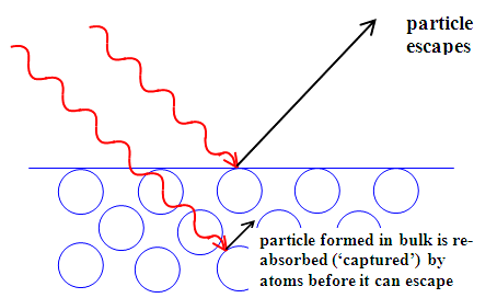
- Surface sensitivity
Nota:
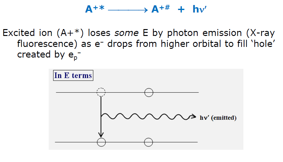
- E.g. XPS is construed to be a ‘surface sensitive’ technique. However, radiation can be derived from few atomic layers of the ‘surface’!
- Surface sensitive technique
more sensitive to atoms near
‘surface’ than atoms in the ‘bulk’.
- should only detect
radiation due to atoms in
the ‘surface’.
- Origin of Surface Sensitivity
- arises from short escape
depth of the emitted ‘particle’
Nota:
- Thus, detector only ‘sees’ particles being emitted from the surface and not from the bulk
- arises from short escape
depth of the emitted ‘particle’
- WHY?
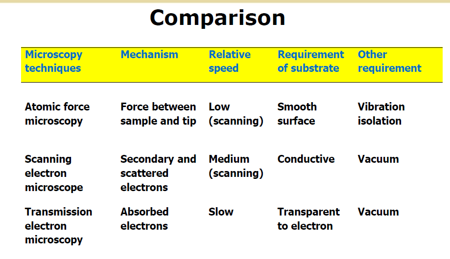
- ELECTRON MICROSCOPY (EM)
- Resolution depends on lambda of
the ‘light’ being used to form the
image:
Nota:
- microscope - imaging device
- (b) EM (5-30 keV -->
lambda ~5 pm) --> ~1
nm (or better!)
- (a) Optical microscope
(visible light, lambda ~ 500
nm) --> ~1 um
- Types
- Scanning (SEMs)
Nota:
- (range --> usually micron)
- Image formation
- processes occur
when electrons
hit a surface
Nota:
- (eV) is a unit of energy ≈1.6×10^−19 joule
- Energy focused by one
or two condenser lenses
to a spot
Nota:
- (ca 0.4 nm to 5 nm in diameter).
- processes occur
when electrons
hit a surface
- operation
Nota:
- can be used for non-conductive samples --> resolution enhanced significantly by sputtering them with conductive metals (e.g. platinum or gold). -Usually for determining the morphologies of surface coatings, solid state samples, ores etc.
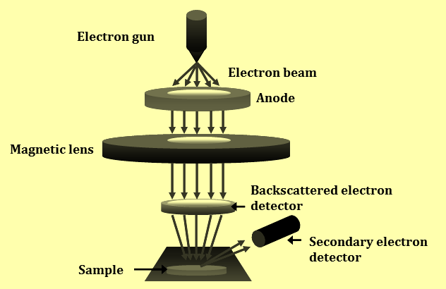
- electron beam - focussed -contact w
the sample - electrons lose energy -
energy exchange -> primary
backscattering & X-rays - detectors
Nota:
- •An electron gun emits a beam which is focused by a series of condenser lens. •Once beam is in contact with sample, the electrons lose energy •Energy exchange resulting in primary back-scattering of electrons. •X-ray is also produced. •Detectors then collect the secondary (electrons emitted by the surface) or backscattered electrons (originated from the beam), and convert them to a signal.
- secondary electron - other
radiation (morphology &
topography)
- primary back-scattered
electron - info on
composition
Nota:
- what is contained inside the material
- Typical configuration
Nota:
- 1.Magnetic lenses rather than optical lenses = more control of magnification. 2.Typically narrow electron beam good depth of field good clarity. 3.10X to 100,000X, maybe even more.
- Can be coupled
with: (EDS or EDX)
Nota:
- Energy-dispersive X-ray spectroscopy
- Difference in energy between
higher/lower energy shell --> X-ray -->
detected by spectrometer
Nota:
- Different element has different atomic structure = different set of peaks on its X-ray spectrum. •Beam ‘excites’ and ‘ejects’ electron in inner shell. •Electrons from higher energy levels to the ‘hole’ until minimum-energy state is regained.
- - give a micrograph
- give % atoms/elements
- Sample prep
- dry
- •‘Sputtering’ for
non-conductive samples
(e.g. biological samples)
--> e.g. thin gold coating
Nota:
- e.g. coating a spider with gold (have to have coat - for interaction w the beam)
- Specimen ‘stub’
- dry
- Examples of output and
applications
Nota:
- •Porous materials •Metal surfaces •Bio-organic material - fungi •Ceramic surfaces •Nanoparticles/nanowires
- Transmission (TEMs)
Nota:
- (range --> usually nano) can look at the atom of the samples- atomic arrangement - the arrays on the surface
- Electrons transmitted
through sample --> magnified
image via a camera.
- Main components
- (1) vacuum chamber (2) emission
source (production of electrons);
(3) Electromagnetic lenses and
electrostatic plates.
- (1) vacuum chamber (2) emission
source (production of electrons);
(3) Electromagnetic lenses and
electrostatic plates.
- Bio samples /
nanotech /
crystallography
- advantage -
higher resolution -
can see atoms
Nota:
- Small wavelengths of high-energy electrons to probe solids at the atomic scale
- disadvantages : 1- selectivity(result
reasonable?) 2- sample damage
under the beam 3- x wet/live sample
- operation
Nota:
- 1.Top of the TEM column electron gun source of electrons. 2.Electrons are accelerated to high energies (ca 100-400 keV) and then focused towards the sample via set of condenser lenses and apertures. 3.Thermionic emission. Thermal energy is added to a material electrons may overcome the energy barrier of the work function and escape. 4.The material used must either have a very high melting point (e.g. W).
- electron beam - focussed -
thermionic emission - (passes
through elements and scatter)
Nota:
- 1.Electrons pass through the specimen and scattered. 2.The information --> converted into an image. 3.One conventional imaging way is to magnify diffraction pattern until it is of the required size for analysis.
- 4.Another way --> fine beam of
electrons is rastered across
the sample --> quantity of
scattering from each point may
be measured separately and
successively.
Nota:
- raster - scan the beam across the sample conventional TEM - spot the beam on the sample
- e.g. output
- metal nanoparticles (Pt)
on nanoporous
material support
Nota:
- What we see in the image is variations in the amount of scattering at different locations in the sample.
- metal nanoparticles (Pt)
on nanoporous
material support
- Other TEM-based/related techniques
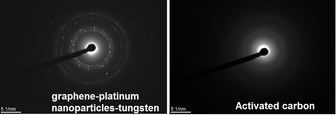
- SAED
Nota:
- Selected-area electron diffraction
- crystallographic information
(selected region)
Nota:
- if the sample is crystal, it difracts
- Diffraction patterns -
electrons scatter
- Crystalline samples --> planes
of atoms that scatter (diffract)
the electrons at specific angles.
Nota:
- what type of crystal is the sample? single crystalline, highly crystalline, polycrystalline amorphous, etc
- •Polycrystalline samples
(or samples with small
particles) = ring patterns.
- •Single crystal samples
= patterns (e.g. spots).
Nota:
- no spots in non-crystalline particles
- •From the ring radii or spot
positions, - determine the
planar spacings.
- Diffraction patterns --> measure
the distances between the atom
planes.
- Basic diffraction pattern
interpretation
Nota:
- e.g. is the sample crystalline or amorphous?
- High resolution
(crystal lattice)
imaging
- Element
distribution
imaging (EFTEM)
Nota:
- (via energy-filtered TEM, EFTEM)
- + with EELS
- generate qualitative or quantitative
elemental maps indicating the location of
specific elements in the sample.
- Create images showing
distribution of selected element
and thickness variation in sample.
- Composition
analysis - EELS
Nota:
- electron energy-loss spectroscopy,
- amt of energy lost by
electrons after they have
passed through a sample is
analysed.
- characterise ENERGY LOSS
- identify the existing element
- EELS spectrum => # of electrons
(intensity) as a function of the
amount of energy they lose
- measure the loss of energy -
converts into a curve - info on
valence states and bonding
- STEM
Nota:
- Scanning TEM imaging
- SAED
- Scanning probe
microscopy
Nota:
- can produce a topograph of the sample (rough?smooth?spiky?) -use mechanical probe instead of electron beam to scan the sample
- Surface topography
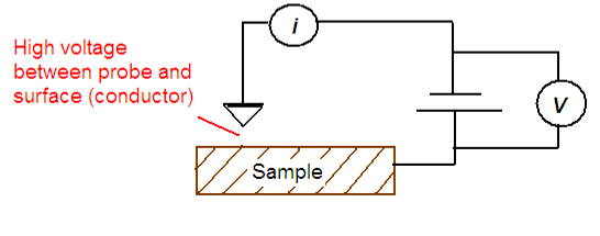
- (STM)
Nota:
- Scanning tunneling microscopy
- general operation
- sample must be
conductive
Nota:
- When the tip is close to surface, a tunnelling current can flow. Relies on the quantum mechanical electron tunneling through an energy barrier larger than its kinetic energy.
- Constant height, d.
- current varies
- current varies
- Measures
surface
electron
density.
Nota:
- when the probe is close to sample, w electric current - sucks up the electron from the sample - when look on the screen, can see the atoms in an array (arranged)
- Constant current, It,
- Tips move up and down;
- Measure tip position (x,y,z)
by piezoelectric device
Nota:
- (Measurement of expansion/contraction (nm) of ceramic material and converting them to an electrical charge) *(1nm ≈ 1V)
- Tips move up and down;
- sample must be
conductive
- QMT
Nota:
- Quantum mechanical tunnelling
- - predicts a finite probability of
electron “tunnelling” through
barrier.
- It ≈ V e^–kd
Nota:
- d = tip/surface separation; k = tunnelling probability (constant) Two modes, namely, (1) constant current, It, (2) constant height, d.
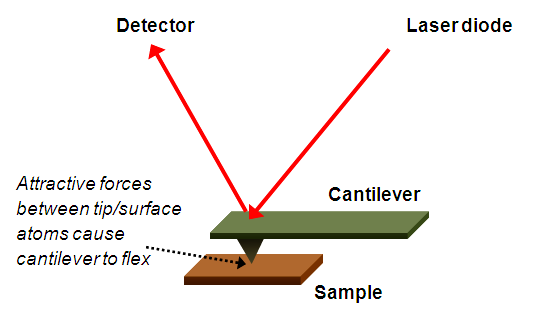
- (AFM)
Nota:
- Atomic force microscopy
- diff from STM ( AFM probe relies on
forces (electrostatic, VDW forces))
--> spring action (Hooke's Law)
- laser diodes measure the
variation of the spring actions
(cantilever)
- Basic
Nota:
- When tip is close to sample surface, forces induced deflection of the cantilever (Hooke's law). Contours of the surface are measured directly using the deflection of the cantilever
- Cantilever = probe (tip)
- Tip radius of curvature = nm
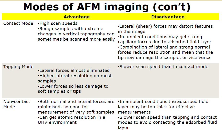
- Imaging Modes
- contact mode - tip
touches and exerts
forces (0.1 – 1 nN)
on the sample.
- tapping mode - the cantilever
tip vibrates near the
resonance frequency at
300kHz. Less destructive than
contact mode
- non-contact mode - the cantilever
oscillates at slightly above the resonant
frequency near the surface of the sample,
but does not contact it.
- contact mode - tip
touches and exerts
forces (0.1 – 1 nN)
on the sample.
- Physical probe scans
specimen by moving sharp
probe in a raster
- Scanning (SEMs)
- diff btwn (AFM & SEM) -
probes and electron
beam
- similarity (AFM &SEM) -
relies on rastering while TEM
(1 electron beam on the
sample)
- Resolution depends on lambda of
the ‘light’ being used to form the
image:
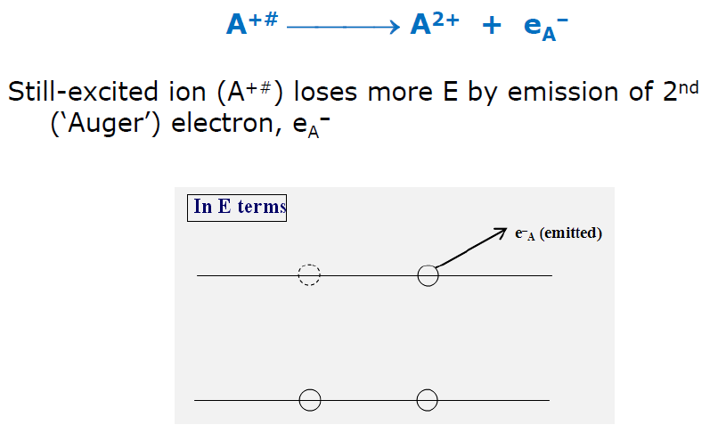
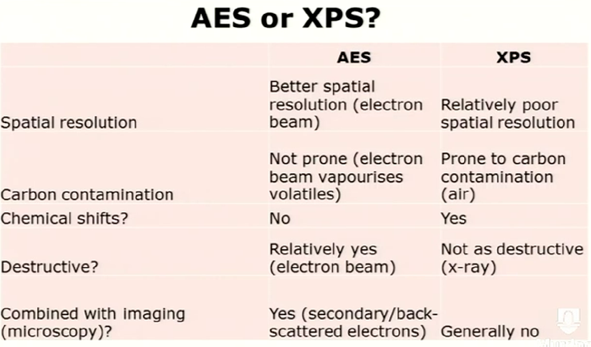
- AES
- Identification and quantification
of elements on materials
surfaces.
- Based upon the measurement of the
kinetic energies of the emitted
electrons
- 3 STEPS
- FEATURES
- photon OR electron beam
- E(e-a) depends only on
E(orbital) - provides
atomic (elemental)
composition
Nota:
- independent of the beam E
- accuracy ~ +-10%
- True surface technique ~ 0.1 – 1 nm,
E(eA–) ~ 20 – 1000 eV (low!) --> v.
short escape depth
Nota:
- very surface sensitive compared to TEM. bcoz the E used is quite low.
- recorded in
differentiated mode
- Little matrix
(chemical shift)
effect
- Auger ‘spot’ size 1–500 um
(good 2-D spatial resolution)
- photon OR electron beam
- APPLICATIONS
- e.g. metallurgy, electronics
- Only limitations are those
of sample
- stable to vacuum
(non-volatile)
- stable to beam
(localized T v. high)
- stable to vacuum
(non-volatile)
- e.g. metallurgy, electronics
- Exploiting the spatial resolution of AES & XPS
- Identification and quantification
of elements on materials
surfaces.
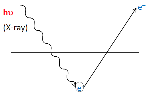
- XPS
Nota:
- a.k.a ESCA - Electron Spectroscopy for Chemical Analysis
- QUANTITATIVE spectroscopy
Nota:
- Spectroscopy = absorption, emission or scattering of light and other radiation by matter, as function of wavelength
- Determines elemental
composition and chemical
state of sample
- Bombards sample w X-ray -> measures the
kinetic energy + # of electrons from surface (< 10
nm). - RELATIVELY SURFACE SENSITIVE
Nota:
- X-ray usually comes from aluminium or magnesium (monochromatic) SURFACE SENSITIVE - things can emerge - photoelectron from K/L shell - eject into the vacuum
- irradiated w PHOTON
Nota:
- E(X-ray or hV) is such that ep– (the ejected ‘photo-electron’) is usually from inner (K or L) shell.
- x-ray less strong than electron
beam - relatively non-destructive -
can analyse sensitive sample e.g.
polymers
- Features
- E(e-p) ~ Ehv - Eb
Nota:
- kinetic energy of emitted electron - E(photoelectron) depends on E(X-ray) & E(binding)-binding energy of electron in atom
- Sensitivity ~0.1 at.% (<
AES); accuracy ~ +-10 %
- Simpler line shape; peaks
identified by element & orbital
of origin, eg, C(1s), S(2p), etc
- Larger spot size
- less surface
sensitive (~1–5 nm)
- Better for
non-conducting
samples
- bigger chemical shift.
Nota:
- Atoms of a higher positive oxidation state --> higher binding energy --> additional coulombic interaction between the photo-emitted electron and nucleus
- UHV
- x detect hydrogen or
helium- orbital diameter
small
- E(e-p) ~ Ehv - Eb
- Chemical Shifts
- Peak positions sensitive to :
a) chemi env b) oxidation
state
Nota:
- contamination in the air- volatile carbon
- chem shift : CH. IN BINDING E of a core
electron of an element due to a CH IN
THE CHEM BONDING of that element.
- Core binding energies
are determined by:
- 1) electrostatic interaction
- 1 REDUCED BY: 2 ) electrostatic
shielding by other electrons
- 3) removal or addition
of electronic charge
- 1) electrostatic interaction
- Withdrawal of valence electron
charge increase in BE
(oxidation)
- Addition of valence
electron charge
decrease in BE
- Chemical shifts in XPS and AES
Nota:
- because: 1- better resolution- finer peak 2- single electron process (AES - 3 energy levels/3 steps)
- XPS better at detecting
chemical shifts
- Peak positions sensitive to :
a) chemi env b) oxidation
state
- Output
- wide scan and
narrowed down
spectra(gives %)
- wide scan and
narrowed down
spectra(gives %)
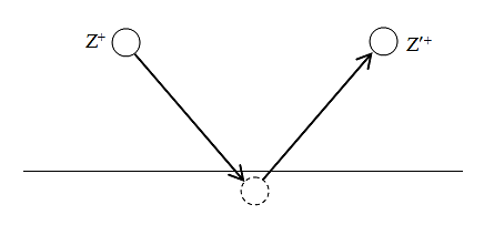
- SECONDARY ION MASS SPECTROSCOPY
- sputters surface of sample with a focused
PRIMARY ION BEAM and collecting and
analyzing ejected SECONDARY IONS.
Nota:
- sputter - shoot something to remove the surface (ions) (some atoms ejected are neutral, but some are ionized) MEASURED SECONDARY IONS BY SPECTROMETER
- determination of elemental,
or molecular composition
- BASIC
- high energy ion beam (5-20 keV)
Nota:
- non reactive ions - He+/Ar+
- Ion beam produced by
bombarding gas with e–
- Focus - Spot size ~ 1–5000 um
- high energy ion beam (5-20 keV)
- ADVANTAGES/FEATURES
- Can determine
all elements
- Sensitivity extremely high ~10^–15
g (NB small volume so only ~ppm
level)
- Microprobe versions
especially powerful (spatial
resolution ~0.5 to 5 um)
- Sampled surface <1 nm
(true surface technique)
- determine +ve & –ve
secondary ions
- Can determine
all elements
- DISADVANTAGES
- Incompatibility between spatial
resolution and sensitivity
- Problems with
differential sputtering
Nota:
- can be uneven spatttering
- expensive
- Incompatibility between spatial
resolution and sensitivity
- sputters surface of sample with a focused
PRIMARY ION BEAM and collecting and
analyzing ejected SECONDARY IONS.
Recursos multimedia adjuntos
¿Quieres crear tus propios Mapas Mentales gratis con GoConqr? Más información.