
Flashcards
Nano
Cards in this deck (30)
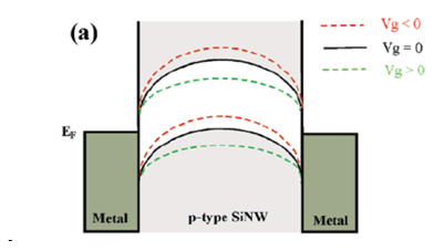
- 1(a) (5 points) Draw the energy band diagram of the p-type Si nanowire (NW) device according to the gate voltage (Vg). Fermi energy (EF) should be indicated on the energy band diagram, and for Vg, if the value is zero, it should be considered positive if negative.
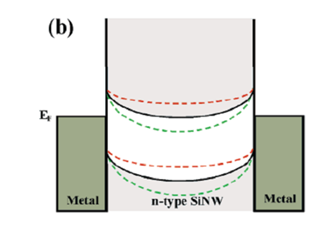
- 2b) (5 points) Draw the energy band diagram of the n-type Si nanowire (NW) device according to the gate voltage (Vg). Fermi energy (EF) should be indicated on the energy band diagram, and for Vg, if the value is zero, it should be considered positive if negative.
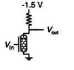
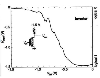
- 3(c) (5 points) An inverter (logic NOT) can be composed with one nanowire (NW). Draw a diagram of how it can be constructed. Explain the operation principle of inverter (logic NOT) based on the diagram.
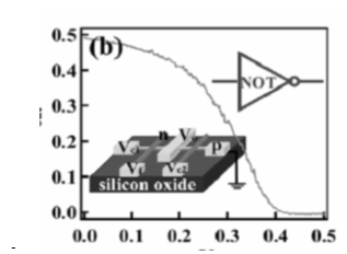
- 4(d) (5 points) When an inverter (logic NOT) composed of one nanowire (NW) is ideally driven, what is the curve of the input voltage (Vin) and output voltage (Vout)?Output-input (V0-Vi) for a nano-inverter configured from two cNW-
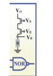
FETs. The inverter has an operation voltage of 0.5 V. - 5a) (5 points) NOR gate can be implemented with carbon nanotube field effect transistors (CNTFETs) and resistor. Draw a circuit of NOR gate composed of CNTFETs and resistor, and indicate the input voltage (Vin), output voltage (Vout) and external voltage on the circuit.
- 6b) (5 points) When the circuit in problem (a) is running, draw the NOR function as the time axis. At this time, logical 0 and logical 1 must be defined.
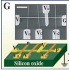
- 7a) (5 points) Draw schematics of logic NOR gate. In Schematics, mark n, p, Vi1, Vi2, Vc1, Vc2, V0 and ground.
- 8(5 points) Draw a symbolic electronic circuit of the logic NOR gate. Mark Vi1, Vi2, Vc1, R, V0 and ground on the symbolic electronic circuit.
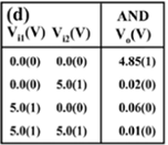
- 9What happens to the experimental truth table of the logic NOR gate?Vo decreases if Vi1 or Vi2 is 1
- 10When the logic NOR gate is logic 0, what state is each of the three transistors constituting the logic NOR gate in? Explain why logic 0 is observed at the logic NOR gate when the three transistors are in that state.The logic-0 is observed when either one or both of the inputs is high. In this case, one or both of the transistors are off and have resistances much higher than the constant resistor, and thus most of the voltage drops across the transistors.
- 11(5 points) When the logic NOR gate is logic 1, what is the state of each of the three transistors constituting the logic NOR gate? Explain why logic 0 is observed at the logic NOR gate when the three transistors are in that state.A logic-1 state can only be achieved when both of the transistors are on; that is, both inputs low.
- 12(5 points) What are the channel material, oxide material, and gate material of the three transistors constituting the logic NOR gate?Logic NOR gates are assembled from 1(p-Si) x 3(n-GaN) cNW-FET arrays.
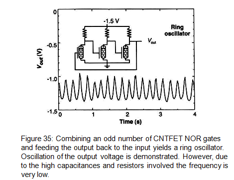
- 13Draw the circuit of a ring oscillator made of the minimum number of carbon nanotubes.
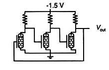
- 14How do we feed to realize the ring oscillator in question?By combining an odd number of inverter elements and feeding the output back to the input, it is possible to realize a ring oscillator
- 15The ring oscillator in question operates at 5 Hz. Draw the oscillation of the output voltage.
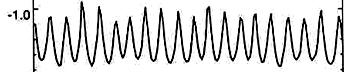
- 16d) (2 points) The frequency of the ring oscillator in question is too low. What is the cause?High capacitances and resistors
- 17By arranging 4 nanowires (NW), a 1x3 crossed NW junction array was made as shown below. Explain how the given 1x3 crossed NW junction array is actually constructed, and draw a schematic diagram of this junction array.Logic NOR gates are assembled from 1(p-Si) x 3(n-GaN) cNW-FET arrays. NOR gates are configured with 2.5 V applied to one cNW-FET to create a constant resistance around 100 megaohms, and with the p-SiNW channel biased at 5 V.
• The two remaining n-GaN NW inputs are used as gates for two cNW-FETs in series. In this way, the output depends on the resistance ratio of the two cNW-FETs and the constant resistor.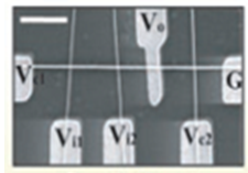
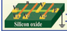
- 18(10 points) Explain the working principle of the given 1x3 crossed NW junction array, and draw the output-input (Vo-Vi) relation.the slope of the data shows that device voltage gain is larger than 5
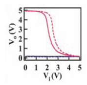
- 19(5 points) Write the truth table of the given 1x3 crossed NW junction array.
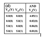
- 20It is possible to make CMOS inverter with n-type carbon nanotube field-effect transistor (CNTFET) and p-type CNTFET. When making a CMOS inverter with back-gate geometry with one carbon nanotube, write down the manufacturing process and draw the final CMOS inverter picture.n-type and p-type CNTFET in series, operated by a common back-gate. Complementary transistors are produced from one single nanotube by doping the section which is not covered by the PMMA resist with potassium
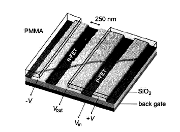
- 21(10 points) Draw the circuit diagram and input-output characteristics of the CMOS inverter. When plotting the input-output characteristics, it is assumed that the voltage gain is 2.
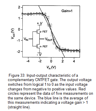
- 22Assume that one ring oscillator is made with three CMOS inverters made of three carbon nanotubes. Simply draw this ring oscillator. Suppose this ring oscillator operates at 5 MHz. Draw the oscillation of the output voltage.If the ring oscillator operates at 5 MHz the frequency will be more spread out.
- 23A pH sensor was manufactured with one nanowire (NW) and the following results were obtained. Explain the configuration and operating principle of a pH sensor using the results below.A Si NW solid state FET whose conductance is modulated by applied gate is transformed into a nanosensor by modifying the silicon oxide surface with 3-aminopropyltriethoxysilane(APTES).
• The APTES provides a surface that can undergo protonation and deprotonation, where changes in surface charge (protonation) chemically gate the Si NW.
• The responses of APTES-modified Si NWs to changes in solution pH demonstrate that the NW conduction increases stepwise with discrete changes in pH from 2 to 9 and that the conductance is constant for a given pH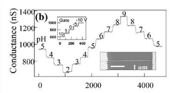
- 24The density of states (DOS) of carbon nanotube and graphene are as follows. Describe what these density of states mean.this illustrates the density of state (DOS) for two zig-zag type CNTs, a (10,0) tube showing a bandgap semiconducting behavior
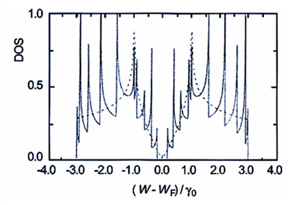
- 25The density of states (DOS) of carbon nanotube and graphene are as follows. Describe what these density of states mean.a (9,0) tube showing no bandgap and, hence, metallic behavior (Figure 9b).
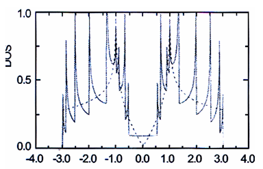
- 265 points) Draw the graphene unit cell and Brillouin zone, and also indicate the axes. Draw a unit vector in the unit cell, and mark K, T, and M points in the Brillouin zone.m is on the midpoint line of top k between 0
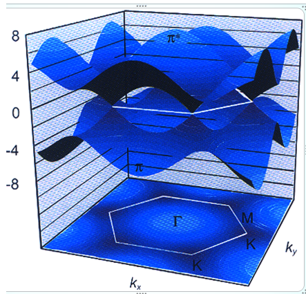
- 27b) (5 points) (3,3) The 3D dispersion relation of CNT was projected onto the first Brillouin zone of graphene. (3,3) Draw the first Brillouin zone in which the allowed states of CNT are indicated, and through this, (3,3) determine whether CNT has metallic or semiconducting properties.first brillouin zone of graphene, K points are allowed states
The fermi level -pi/P and pi/P indicate metallic behavior of this tube.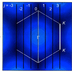
- 28derive:- When ky=0, kx=+- 4pi/3a
- The roll-up by the chiral vector Ch leads to periodic boundary conditions in the circumferential direction. Ch*k=2pi*j
ch= sqrt(3)a
k= 2pij/9ysqrt3)a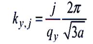

- 29equation for the graphene 2-D energy state.
- 30(10 points) (3,3) The 3D dispersion relation of CNT was projected onto the first Brillouin zone of graphene as shown below. What is the first Brillouin zone? What about Allowed states? What is the energy gap at point k and point T?There is no energy gap at point k, and at point T is 8/3 ev.
Information
- Description
- Flashcards on Nano, created by Tony Shin on 16/06/2021.
- Created by
- Tony Shin · Jun 2021
- Updated
- Jun 17, 2021
- Views
- 10
- Rating