608685
Part 2: Electrons in Solids
- Weak binding (FEM)
- Tight binding
- Energy band structure
Annotations:
- - Arises from both models. - Energy gap increases with Vo. - Position of Ef is determined by the number of valence electrons per unit cell.
- Insulators (Large energy gap,
Ef inside it, no Fermi surface)
- Semiconductors: small energy gap,
Ef inside it, no Fermi surface
- Metals: Ef is inside energy band
Annotations:
- Away from edge, FEM holds
- Brillouin zones
Annotations:
- A BZ contains a set of wavevectors which spans the space of all wavevectors which can be scattered by the crystal. All wave vectors in other BZ's satisfy k'=k+G (Laue's condition), where G is a reciprocal lattice vector.
- Different BZ's correspond
to different energy bands
Annotations:
- Energy gaps coincide with BZ boundaries (surfaces) Energy bands lie in different BZs
- 3 Zone schemes
- Extended
- Periodic
- Reduced
- Extended
Annotations:
- As an electron jumps from the valence band to the conduction band, a positively charged hole is left. Same properties as electron but positively charged!
- Energy band structure
- Density of charge carriers in semiconductors
(IMPORTANT DERIVATION!
- Density of states (TO REMEMBER)
- Occupation number
(FD distribution) (TO REMEMBER)
Annotations:
- Remember to approximate with simple exponential as the exponential in the denominator becomes >> 1
- Of electrons f_FD
- Of holes: 1-f_FD
(remember to rearrange)
- Change variable and integrate to get Number
of charge carriers + multiply by 2 for spin
- K and Real space diagrams for
charge carrier densities
- Electrons are in conduction band minima
- Holes are in valence band maxima
- Electrons are in conduction band minima
- Product of n and p only
depends on energy gap E_g.
- For intrinsic semiconductors
n=p=n_i=p_i
Annotations:
- e.g. Ge, Si, GaAs
- n=p=n_i=p_i=sqrt(np)
are fully specified by E_g
- Extrinsic semiconductors. Dopants:
donors have valence >; acceptors have
valence < (donate holes)
- Have extrinsic carriers from dopants
- Usually dopant density >> intrinsic density =>
dopants dominate conduction properties at normal T's
- Usually dopant density >> intrinsic density =>
dopants dominate conduction properties at normal T's
- n-type semiconductors:
electrons = majority carriers;
holes = minority carriers
- p-type semiconductors:
holes = majority carriers;
electrons = minority carriers
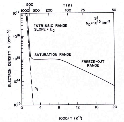
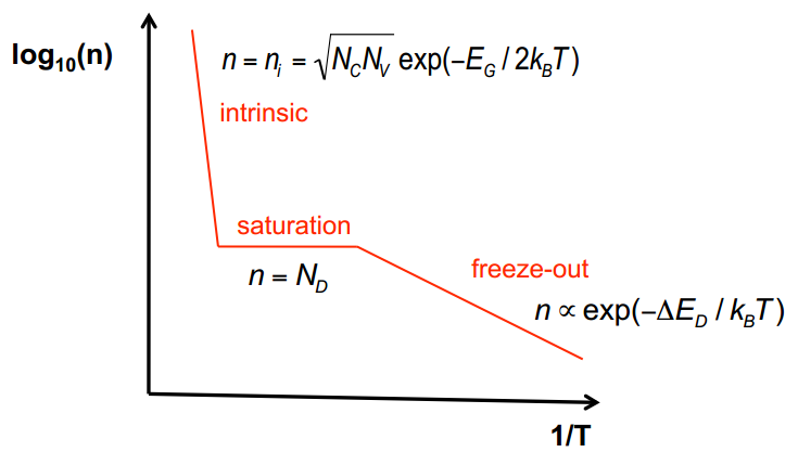
- Temperature dependence of
conductivity
- At low T: extrinsic carriers are frozen out,
Intrinsic carriers dominate
- In saturation region (T about 300K): dopants are
fully ionised and dominate conduction properties.
This is the operating range of the device.
- At T>>300K semiconductor ionises and intrinsic carriers dominate
- At low T: extrinsic carriers are frozen out,
Intrinsic carriers dominate
- Temperature dependence of
conductivity
- Insulators have no dopants
- Have extrinsic carriers from dopants
- For intrinsic semiconductors
n=p=n_i=p_i
- n = N_c*e^((E_c-E_f)/k_b*T)
- dn/dx = -(dE_c/dx)*n/k_b*T
- dn/dx = -(dE_c/dx)*n/k_b*T
- K and Real space diagrams for
charge carrier densities
- Change variable and integrate to get Number
of charge carriers + multiply by 2 for spin
- Holes: empty states in
otherwise filled bands
- Density of states (TO REMEMBER)
- Bloch States: - 2 separate
bands for conduction and
valence. - Use m*
- Derivation of m*
- Derivation of m*
- FEM: - dispersion relation is
a parabola on which states lie.
- Use m
- Conduction in semiconductors
- In FEM
- Filled states form a
Fermi sphere in k-space
Annotations:
- Radius k_f of the sphere was derived in Part 1 of the course.
- k is related linearly to momentum
and velocity of electrons
- For each electron going in +k there is
one in -k => no net current
- Apply E field
- Use De Broglie relation to express
dk = (-eE/h_bar)dt
- Now electrons are shifting to higher k values
=> Fermi sphere is moving => current
- Scattering slows down the increase in velocity
of Fermi sphere by knocking electrons back to
empty states in the valence band
Annotations:
- Electrons at the leading edge (in the Fermi sphere, k.-space) are scattered back to the opposite edge.
- Given a scattering time t, dk/dt settles down at -(eE/h_bar)t
=> Steady State
- Drift velocity: v_drift = (eE/m)t
of all electrons in the sphere
Annotations:
- where et/m = u (carrier mobility)
- Drift velocity: v_drift = (eE/m)t
of all electrons in the sphere
- Scattering slows down the increase in velocity
of Fermi sphere by knocking electrons back to
empty states in the valence band
- Now electrons are shifting to higher k values
=> Fermi sphere is moving => current
- Energy of level E_c = -eV + const. Moreover: E_field = -dV/dx
- Hence, dE_c/dx = -edV/dx = e*E_field
- dn/dx = -e*E_field*n/k_b*T
- Einstein's relation: D_n/u_n = k_b*T/e
- Einstein's relation: D_n/u_n = k_b*T/e
- dn/dx = -e*E_field*n/k_b*T
- Hence, dE_c/dx = -edV/dx = e*E_field
- Use De Broglie relation to express
dk = (-eE/h_bar)dt
- For each electron going in +k there is
one in -k => no net current
- Filled states form a
Fermi sphere in k-space
- In real solids same thing except that
- m* instead of m and have + sign for holes
- Charge transport occurs separately in
the valence and in the conduction band
- Collisions can knock electrons to other
band or other state in the same band
- Different sources of scattering
Annotations:
- Temperature dependent: - Scattering from acoustic and optical phonons, dominates at high temperatures. - Scattering from ionised donor centres. Important for devices. Temperature independent: - Scattering from crystal defects, dominates at low temperatures.
- T dependent: phonons, ionised dopant centres
- T independent: crystal defects
- Different sources of scattering
- Charge carrier mobility: defined as
ratio of drift velocity to applied E
- Can also be expressed as u = et/m* (careful
with sign for different charge carriers!)
- Can also be expressed as u = et/m* (careful
with sign for different charge carriers!)
- m* instead of m and have + sign for holes
- Drift: charge flow due to E field
Annotations:
- Note: holes move in same direction as current, electrons in opposite.
- Drift current density: Jn = qnv = enuE (for e's)
and Jp = qpv = qpu_pE (for holes)
- Total drift current density is given by the sum
J_drift = Jn + Jp = e(qpu_p + qnu_e)E
- Define conductivity sigma = e(qpu_p + qnu_e)
such that J = sigma E
Annotations:
- Ohm's Law
- Total current is sum of drift and diffusion currents
J_n = e*n(x)*u_n*E_field + e*D_n*dn/dx
Annotations:
- Note: total current J must be costant (in most cases) everywhere according to Kirchoff's laws.
- In equilibrium: Jn and Jp are both equal to 0
=> e*n(x)*u_n*E_field = - e*D_n*dn/dx
- Define conductivity sigma = e(qpu_p + qnu_e)
such that J = sigma E
- Total drift current density is given by the sum
J_drift = Jn + Jp = e(qpu_p + qnu_e)E
- Diffusion: proportional to gradient of carrier concentration:
phi_n(x) = -D_n dn/dx || Phi_p(x) = D_p dp/dx
- D's are diffusion coefficients (units m^2 s^-1)
- Diffusion currents: J_n = e*phi_n(x) = e*D_n*dn/dx
J_p = e*phi_p(x) = -e*D_p*dp/dx
- If δn charge carriers are injected in region of opposite type:
δn(x) = Δ n exp( − x L n )
- D's are diffusion coefficients (units m^2 s^-1)
- Generation and recombination of elctron-hole pairs
- At equilibrium: the two occur at the same rate
- Non equilibrium: minority carriers, electrically or optically created,
recombine with some majority carriers. The recombination time is
inversely proportional to the number of majority carriers.
- Number of excess minority carriers decays exponentially
in time at a rate equal corresponding to recombination time "tau".
- Diffusion Length: how long charge carriers propagate before
they recombine. L_n = sqrt(D_n*tau_n). The number of excess
carriers decays exponentially at a decay length L_n
- Number of excess minority carriers decays exponentially
in time at a rate equal corresponding to recombination time "tau".
- At equilibrium: the two occur at the same rate
- In FEM
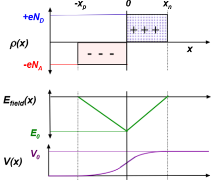
- pn-junction formation: take n and p-type and
place them next to each other
Annotations:
- Lecture 19
- Diffusion causes majority carriers to move
from both sides to the opposite side
- A net charge density of opposite sign remains on each side
in the depletion region => Efield is generated across junction
- Approximate charge density as constant
on each side of depletion region
Annotations:
- i.e. graph charge vs displacement is a rectangle on each side. rho = e*N_D
- When diffusion and drift balance => Equilibrium
=> E_f is constant everywhere
- Use Gauss's Law to work out field in the depletion region
Annotations:
- Integrate in p (-x to 0) and n (0 to x) regions separately. At interface take E = E_0. Express E_0 in terms of boundary conidtions at edges taeking and E = 0 at the edges (x_n and x_p).
- Integrate E field to get the potential
- Use boundary conditions V(x_n) = V_0 and V(x_p) = 0 to
work out V in p and n (up to constant V_0) regions
- Impose continuity of V at boundary to express V_0 as function of x_p and x_n
- Use relations for x_p and x_n to express V_0 as a
function of the width of the depletion region
- E_v= -eV and E_c = E_v + E_g
- E_v= -eV and E_c = E_v + E_g
- Use relations for x_p and x_n to express V_0 as a
function of the width of the depletion region
- Impose continuity of V at boundary to express V_0 as function of x_p and x_n
- Use boundary conditions V(x_n) = V_0 and V(x_p) = 0 to
work out V in p and n (up to constant V_0) regions
- Obtain expression for relative width of p and n region in
terms of carrier concentrations from continuity of >E at
interface
- Rearrange to get x_p and x_n in terms of width
W and carrier concentrations
- Rearrange to get x_p and x_n in terms of width
W and carrier concentrations
- Use Gauss's Law to work out field in the depletion region
- Approximate charge density as constant
on each side of depletion region
- A net charge density of opposite sign remains on each side
in the depletion region => Efield is generated across junction
- Operational behaviour of pn-junctions.
Can bias this voltage in 4 ways
Annotations:
- Lecture 20
- Reverse bias -V: step
increases, W increases
- Zero bias. E_f is constant
- Forward bias +V: step decreases, W decreases
the two E_f's are separated by eV
- Flat band V=V_0: step is 0, W=0,
difference between E_f's is eV_0.
- Proof of Shockley's Ideal Diode Equation
Annotations:
- to follow
- Calculate excess minority carriers Δp_n from difference
between p_n and p_n(x_n) (same for n)
Annotations:
- for p_n, use fermi level of n region. for p_n(x_n), use fermi level of p region. Δp_n = p_n *(exp(ev/kT)-1)
- Consider diffusion of minority carriers δp_n(X)=Δp_n*exp(-X/L_p) ,
Annotations:
- X = x-x_n
- Hence diffusion current J_diff = e*D_p/L_p*Δp_n*exp(-X/L_p)
- Set X = 0, so no recombination takes place. Considering both p and
n diffusion currents and multiplying by area.
- Shockley's Equation for ideal diodes: I =
e*A*[D_p/L_p*p_n +
D_n/L_n*n_p]*(exp(eV/kT) -1)
Annotations:
- Fails for voltages above flat band. Neglects recombination within depletion region.
- Devices
- Forward bias
- Diode (one-way current gate)
- LED: recombination generates photons
- Diode (one-way current gate)
- Zero-bias
- Photovoltaic-cells: photon absorption
generates carriers which create voltage
- Photovoltaic-cells: photon absorption
generates carriers which create voltage
- Reverse-bias
- Photodiodes: light absorbed generate
carriers which generate current
- Photodiodes: light absorbed generate
carriers which generate current
- Forward bias
- Shockley's Equation for ideal diodes: I =
e*A*[D_p/L_p*p_n +
D_n/L_n*n_p]*(exp(eV/kT) -1)
- Set X = 0, so no recombination takes place. Considering both p and
n diffusion currents and multiplying by area.
- Absorption and emission in semiconductors
- TO CLARIFY: ABSORPTION COEFF'S ETC.
- Horizontal transition (big shift in k)
- Non-radiative: phonons
- Phonons carry a lot of momentum, but little energy
- Phonons carry a lot of momentum, but little energy
- Non-radiative: phonons
- Vertical transition (energy band jump)
- Radiative: photon
- Photons carry little momentum
but a lot of energy
- Photons carry little momentum
but a lot of energy
- Non-radiative: multiphonons (large change in k)
- Requires hole and electrons with same k
Annotations:
- Hole and electrons have same k, so that direct transition is possible
- For direct gap semiconductors
this occurs directly
- Direct gap s.c. suitable for optical purposes
- Emission occurs at E_g
- Absorption only occurs at energies >= E_g, hence lower energies get
through and show colour of material, while higher energies are absorbed.
- Direct gap s.c. suitable for optical purposes
- For indirect gap semiconductors requires previous
horizontal transition: extremely unlikely
- Indirect gap s.c. not suitable for optical purposes
- Indirect gap s.c. not suitable for optical purposes
- Radiative: photon
- TO CLARIFY: ABSORPTION COEFF'S ETC.
Media attachments
Want to create your own Mind Maps for free with GoConqr? Learn more.