
Quiz
Electronics
Create a free account to finish this quiz
Save your progress and see your final score.
Already have an account? Sign in
Questions in this quiz (7)
1Select all of the following that are true.
- Ap-type silicon is created by adding acceptor impurities that have 3 valence electrons.
- Bfor p-type silicon, a large number of extra holes are created in the valence band, without creating corresponding free electrons in the conduction band.
- Cp-type silicon is created by adding donor impurities that have 5 valence electrons.
- Dp-type silicon has an overall positive charge.
2Select all of the following that are true.
- An-type silicon is created by adding donor impurity atoms that have 5 valence electrons.
- Bfor n-type silicon, a large number of extra free electrons are created in the conduction band, without leaving holes behind in the valence band.
- Cn-type silicon is created by adding acceptor impurity atoms that have 3 valence electrons.
- Dn-type silicon has an overall negative charge.
3Which of the following best describes the operation of a p-channel JFET?
- AA positive voltage applied to the gate creates an electron inversion layer that creates a channel connecting the source and drain.
- BA negative voltage applied to the gate creates a hole inversion layer that creates a channel connecting the source and drain.
- CAs the gate voltage becomes more positive, the depletion region around the gate widens, which narrows the channel until pinchoff is reached.
- DAs the gate voltage becomes more negative, the depletion region around the gate widens, which narrows the channel until pinchoff is reached.
4What is the effect of the emitter resistor RE in the amplifier circuit below? (Select all answers that apply)
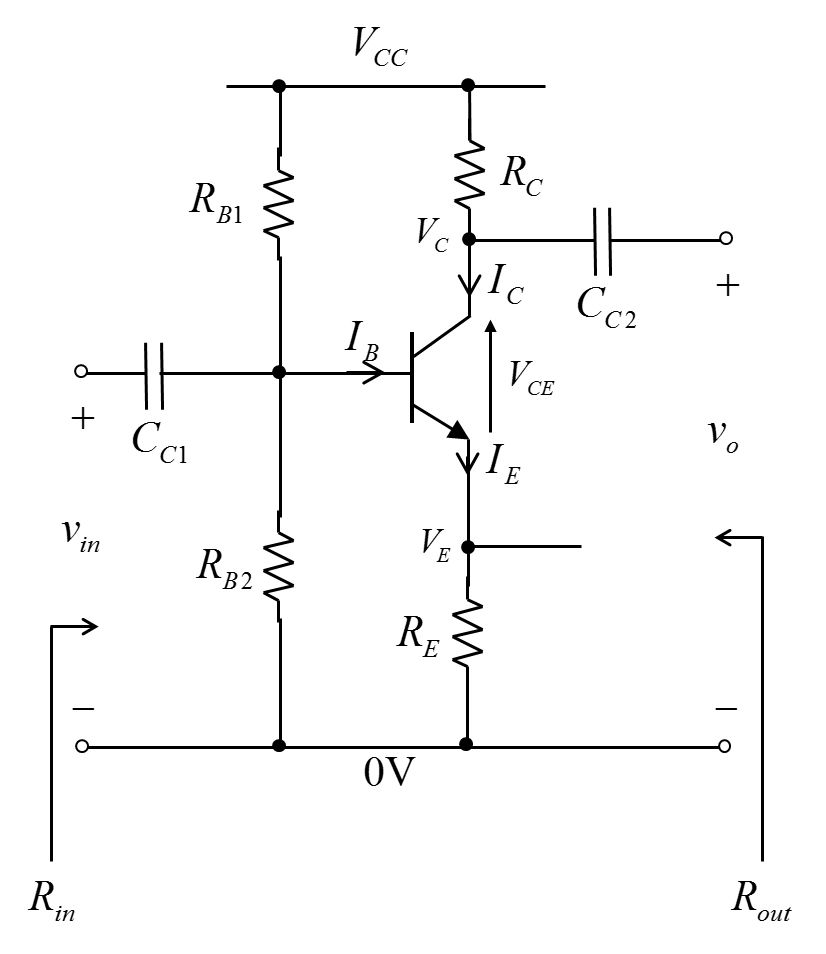
- AIncreases the input resistance, Rin.
- BStabilises the boas point with respect to changes in transistor β
- CIncreases the small signal gain, vo/vin.
- DDecreases the small signal gain, vo/vin.
- EDecreases the input resistance, Rin.
5In the circuit below, what is stage T2 called? (select all that apply)
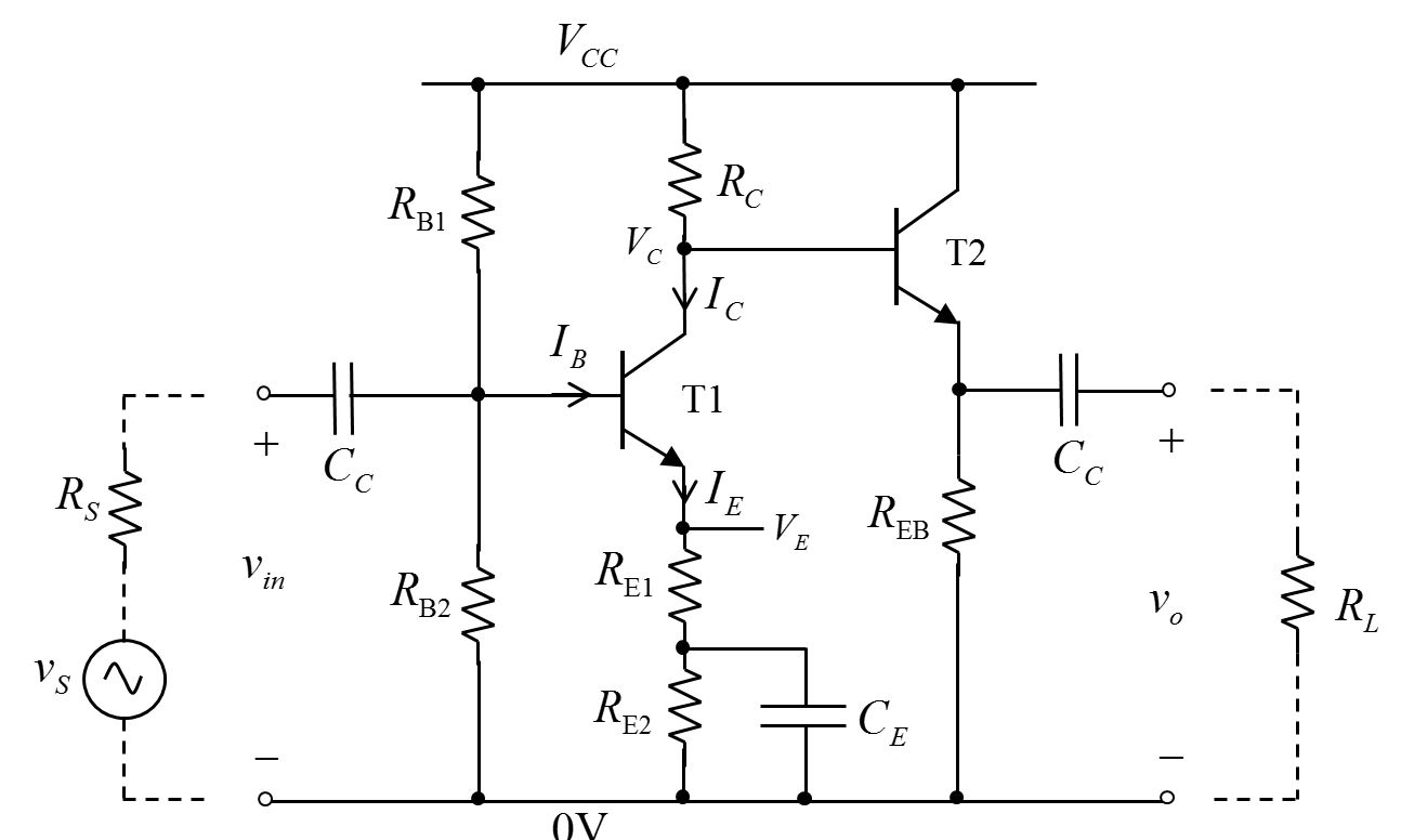
- AA common source stage
- BA common drain stage
- CA common gate stage
- DA source follower
- EAn emitter follower
- FA common collector stage
6In the circuit below, what is stage T2 called? (select all that apply)
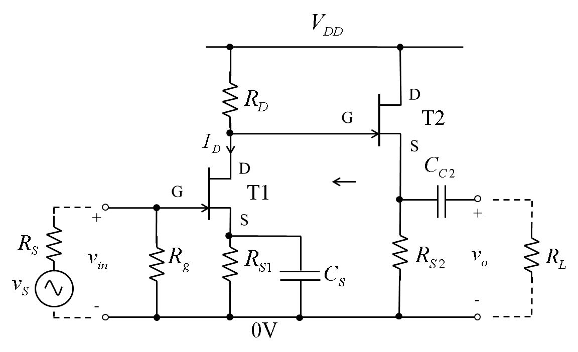
- AA common source stage
- BA source follower
- CA common drain stage
- DA common gate stage
7A gated D Latch is shown below. Which of the following is true?
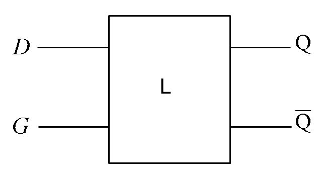
- AThe Q output toggles if one of the inputs is held high.
- BThe Q output follows the D input when G = 1.
- COnly one of the inputs can be high at a time.
- DThe Q output becomes equal to the value of D only on the rising edge of G.
Information
- Description
- Quiz on Electronics, created by Joey Arvi on 10/11/2018.
- Author
- Joey Arvi
- Language
- English
- Views
- 4
- Rating
- No ratings yet Rate this quiz