
Quiz
1-69+1-6
This quiz has question types that open in the usual player.
Questions in this quiz (76)
1α is the ratio of [blank_start]collector[blank_end] current to [blank_start]emitter[blank_end] current
- Acollector
- Bemitter
2β is the ratio of [blank_start]collector[blank_end] current to [blank_start]base[blank_end] current
- Acollector
- Bbase
3A BJT is said to be operating in the saturation region if [blank_start]both junctions are forward biased[blank_end]

- Aboth junctions are forward biased
4A BJT is said to be operating in the active region, then explain why the amount resistance is low in base emitter junction?
[blank_start]forward bias[blank_end]- Aforward bias
5A cross-section of a conventional integrated circuit n-p-n bipolar transistor is shown in Figure. Identify and write the answer of the number 1.
[blank_start]base[blank_end]
- Abase
6A cross-section of a conventional integrated circuit n-p-n bipolar transistor is shown in Figure. Identify and write the answer of the number 2.
[blank_start]emitter[blank_end]- Aemitter
7A cross-section of a conventional integrated circuit n-p-n bipolar transistor is shown in Figure. Identify and write the answer of the number 3.
[blank_start]collector[blank_end]- Acollector
8A full-wave rectifier circuit is represented in Figure. Identify the output frequency of the given circuit?
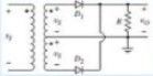
- AFrequency of the output voltage of full-wave rectifier is twice of frequency of its input voltage
- BFrequency of the output voltage of full-wave rectifier is one-half of frequency of its input voltage
- CFrequency of the output voltage of full-wave rectifier the same of frequency of its input voltage
9A half-wave rectifier circuit is represented in Figure. Identify N1 and N2
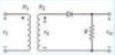
- AN1 and N2 are the positively charged vacancy in the forbidden band
- BN1 and N2 are the number of primary and secondary turns respectively
- CN1 and N2 are the positively charged vacancy in the conduction band
10An idealized n-p-n bipolartransistor biased in the forward-active mode is shown in Figure. Identify bias for each junction.

- ABE - forward biased, BC - forward biased
- BBE - reverse biased, BC - reverse biased
- CBE - reverse biased, BC - forward biased
11A JFET has high input impedance because ……..
- Ait is made of semiconductor material
- Binput is reverse biased
- Cof impurity atoms
- Dnone of the above
12A JFET has ____ power gain.
- Avery small
- Bsmall
- Cnone of the above
- Dvery high
1313.A MOSFET has many terminals?
- A3
- B3 or 4
- C2 or 3
- D4
1414.A p-n junction diode is under various battery supply connection is shown in Figure. Show the figure, which illustrates a diode under reverse bias.
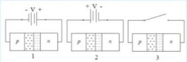
- A1
- B2
- C3
15A p-n junction diode is under various battery supply connection is shown in Figure. Show the figure, which illustrates a diode under zero bias.
- A1
- B2
- C3
16A p-n junction diode is under various battery supply connection is shown in Figure. Show the figure, which illustrates a diode under forward bias.
- A2
- B1
- C3
17A transistor may be used as a switching device or as a (you used it in Lab 4) [blank_start]potentiometer[blank_end]
- Apotentiometer
18A zener diode is a type of junction diode that is normally used in ____
- Acurrent regulator circuits
- Bvoltage multiplier circuits
- Cvoltage regulator circuits
- Dvoltage divider circuits
19A zener diode voltage regulator circuit is shown in Figure. If source voltage increases, then identify Iz and Iload?

- AIz will increase. Iload will remain unchanged
- BIz will decrease. Iload will increase
- CIz will remain unchanged. Iload will increase
20An energy band diagram is presented in Figure. How do differentiate semiconductors, conductors on the basis of band gap?

- AThe distinction between conductors, insulators and semiconductors is largery concerned with the relative width of the valence energy gaps in their energy band structures.
- BThe distinction between conductors, insulators and semiconductors is largery concerned with the relative width of the forbidden energy gaps in their energy band structures.
- CThe distinction between conductors, insulators and semiconductors is largery concerned with the relative width of the conduction energy gaps in their energy band structures.
21An N-P-N transistor ciruit in the common-emitter configuration is shown in Figure. Explain why this circuit is called common-emitter configuration?
[blank_start]the emitter is the common connection[blank_end]
- Athe emitter is the common connection
22An N-P-N transistor will be off state when Vb and Ve ? So identify relationship between them.
[blank_start]equal[blank_end]- Aequal
23An N-P-N transistor will be on state when Vb and Ve ? So identify relationship between them.
[blank_start]Ve more than Vb[blank_end]- AVe more than Vb
24As you know input impedance of JFET is high and in this case the input current is ___.
[blank_start]very small[blank_end]- Avery small
25As the forward voltage increased for Vf < V0 why in the VI curve the forward current If almost zero?
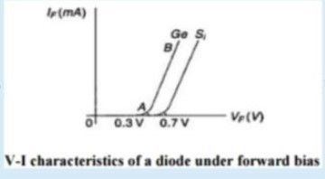
- Abecause the potential barrier in the forward bias increases
- Bbecause the potential barrier prevents the holes from P region and electrons from N region to flow across the depletion region in opposite direction
- Cthe potenial barrier at the junction completely disappears and hence, the holes cross the junction from P to N type and electrons cross the junction to opposite direction, rsulting large current flow in external circuit.
26The cut in voltage or threshold voltage Vf below which the current is very small. At this voltage the potential barrier is overcome and the current through the junction starts to increase rapidly as shown in Figure. Explain why it happens
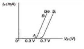
- Abecause the potential barrier at the junction completely dissappears and hence, the holes cross the junction from P to N type and electronics cross the junction to opposite direction, resulting large current flow in external circuit.
- Bbecause the potential barrier in the forward bias increases.
- Cbecause the potential barrier prevents the holes from P region and electrones from N region to flow across the depletion region in opposite direction.
27At cut-off, the JFET channel is ….
- Aa completely closed by the depletion region
- Bat its widest point
- Cextremely narrow
- Dreverse biased
28At using of such rectifier the time diagram of output voltage will be:
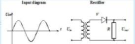
- A
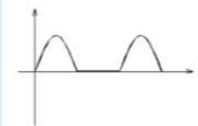
- Banother
- Canotherr
- A
29Below is shown circuit symbol of an operational amplifier. Identify the meaning of number 4.

- AHigh power supply terminal
- BInverting terminal
- CNon-inverting terminal
- DOutput terminal
- ELow power supply terminal
30Both NPN and PNP transistors show ___________ gain.
- AVoltage
- BPower
- CCurrent
31By using settings window for the enhancement type n-MOSFET identify a particular voltage which needs to a conducting channel.

- A3.4386 V
- B3.4286 V
- C3.4486 V
32Calculate the current through the diode
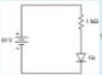
- A9.5mA
- B9mA
- C10mA
33Calculate the unknown values of the diode in the circuit shown in Figure in the following question - The voltage drop across the diode is known. It is 0.7 V for silicon and 0.3 V for germanium. ("Si" near the diode means it is silicon.) Write down the diode voltage drop Vd = ________________________ and find the voltage drop across the resistor Vr?

- AVd=0.7V, Vr=4.3V
- BVd=0.3V, Vr=4.3V
- CVd=0.7V, Vr=0.3V
34Choose the correct statement
- AMOSFET has high value of on-state resistance as compared to other devices
- BMOSFET has lower switching losses as compared to other devices
- CMOSFET suffers from secondary breakdown problems
- DAll of the mentioned
35Component in a clapping circuit which acts as a battery
- Ainductor
- Btransformer
- Cresistor
- Dcapacitor
36Conductivity in semiconductors due to the presence of_________carriers.
- Amobile("free")
- Bminor
- Cimmobile
37Construct the given file below. Choose any pnp transistor in your Proteus.

- A

- B*try to remember the pic*
- A
38Construct the given file below. Choose any pnp transistor in your Proteus.

- A

- B*try to remember the pic*
- A
39Define a hole in a semiconductor?
- Apositively charged vacancy in the forbidden band
- Bpositively charged vacancy in the conduction band
- Cpositively charged vacancy in the valence band
40Define a zero bias p-n junction?
- Awhen an inernal voltage is applied
- Bwhen no external voltage is applied
- Cwhen an external voltage is applied
41Define the condition when the saturation region occurs fo the n-channel JFET
- AVds>Vds(sat)
- BVds>=Vds(sat)
- CVds<=Vds(sat)
42Define what is a full-wave rectifier circuit?
- Aa rectified output voltage occurs during both the positive and negative cycles of the input signal
- Ba rectified the output voltage appears only during the positive cycle of the input signal
- Ca rectified the output voltage appears only during the negative cycle of the input signal
43Define what is a half-rectifier circuit?
- Aa rectified output voltage occurs during both the positive and negative cycles of the input signal
- Ba rectified the output voltage appears only during the positive cycle of the input signal
- Ca rectified the output voltage appears only during the negative cycle of the input signal
44Define what is rectifier?
- ADevice which converts dc voltage into an alternating (ac) voltage
- BDevice which generates dc voltage
- CDevice which converts alternating (ac) voltage into an dc voltage
45Determine cut off frequency from the given circuit?

- A4825.3 Hz
- B3825.3 Hz
- C2825.3 Hz
46Diagram of an electronic power supply is presented in figure. Define why is using a voltage regulator in rectifier circuits.
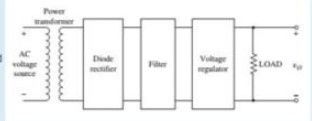
- AIt absorbs a constant voltage level
- BIt maintans a constant voltage level
- CIt generates a constant voltage level
47Diagram of an electronic power supply is presented in figure. Define why is using a filter regulator in rectifier circuits.
- AIt absorbs pulsating output of rectifier into a steady dc level
- BIt generates pulsating output of rectifier into a steady dc level
- CIt converts pulsating output of rectifier into a steady dc level
48Diodes are made to dissipate a certain amount of power, and this is quoted as a maximum power rating
- A2.86 A (Provided the current in the circuit does not exceed this, the diode will not overheat and burn out.)
- B2.75 A (Provided the current in the circuit does not exceed this, the diode will not overheat and burn out.)
- C2.56 A (Provided the current in the circuit does not exceed this, the diode will not overheat and burn out.)
49Diode limiter in which diode is forward biased during negative attenuation has anode connected to
- Aground
- Binput
- Coutput
- Dfront
50Diodes are made to dissipate a certain amount of power, and this is quoted as a maximum power rating in the manufacturer's specifications of the diode. Assume a silicon diode has a maximum power rating of 2 watts. How much current can it safely pass?
- A2.56
- B2.86
- C2.75
51During positive half cycle of total secondary voltage of bridge rectifier, number of diodes forward biased are
- Atwo
- Bthree
- Cfour
- Done
52Electron and hole currents in p-n-p bipolar transistor biased in the forward-active mode shown in Figure. Explain the flow of the iB component of the base current.

- AiB, comes from electrons flowing from the base into the emitter as a result of the reverse-biased E-B junction
- BiB, comes from electrons flowing from the base into the emitter as a result of the forward-biased E-B junction
- CiB, comes from electrons flowing from the emitter into the base as a result of the forward-biased E-B junction
53Electron and hole currents in p-n-p bipolar transistor biased in the forward-active mode shown in Figure. Explain the total base curent.
- Athe total base current in the p-n-p device is an exponential function of the B-B voltage.
- Bthe total base current in the p-n-p device is an exponential function of the E-B voltage.
- Cthe total base current in the p-n-p device is an exponential function of the C-B voltage.
54Electron and hole currents in p-n-p bipolar transistor biased in the forward-active mode is presented in Figure. Named the two current loops in this transistor.

- AThe base curent loop and the collector current loop.
- BThe emitter curent loop and the collector current loop.
- CThe base curent loop and the emitter current loop.
55Electron and hole currents in p-n-p bipolar transistor biased in the forward-active mode is presented in Figure. Explain the flow of the Ib component of the base current.

- Athe iB component of the base current will be the same as the collector current.
- Bthe iB component of the base current will be much smaller as the collector current.
- Cthe iB component of the base current will be much higher as the collector current.
56Explain the condition, which is known as pinch-off for a p-channel JFET
[blank_start]If a larger positive gate voltage is[blank_end] [blank_start]applied, the condition can be achieved[blank_end]- AIf a larger positive gate voltage is
- Bapplied, the condition can be achieved
57Explain the given I-V curve
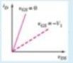
- Aa small reverse-biased gate voltage
- Bzero gate voltage
- Ca gate voltage that achieves pinchoff
58Explain the given I-V curve

- Azero gate voltage
- Ba small reverse-biased gate voltage
- Ca gate voltage that achieves pinchoff
59Explain when and in which region, the ideal curent-voltage characteristics of JFET are described by
[blank_start]when the transisotr is biased in the[blank_end] [blank_start]saturation region[blank_end]
- Awhen the transistor is biased in the
- Bsaturation region
60Explain why only the inductor or the capacitor alone is not used
- AIn inductor filter Ripple factor is inversely propotional to load, in capacitor filter Ripple factor is propotional to load, so in LC filter ripple factor will be independent of load
- BIn inductor filter Ripple factor is propotional to load, in capacitor filter Ripple factor is propotional to load, so in LC filter ripple factor will be independent of load
- CIn inductor filter Ripple factor is inversely propotional to load, in capacitor filter Ripple factor is inversely to load, so in LC filter ripple factor will be dependent of load
61Explain why the p-channel JFET is generally called a lower frequency device than the n-channel JFET?
- ABecause holes flow in the channel from the source to the drain
- BBecause the n-channel acts essentially as a resistance
- CBecause hole mobility is lower than electron mobility
62If family Id versus Vds curves for an n-channel enhancement-mode MOSFET is shown in Figure. Explain the Vds(sat) voltage?

- Athe gate voltage and vertical electric field increase, the carrier mobility decreases. This result, again, directly influences the current-voltage characteristics of the device.
- Bthe Vds(sat) voltage is a single point on each of the curves. This point denotes the transition between the nonsaturation region and the saturation region.
- CA positive gate voltage is required to turn the device off.
63Figure 6-1 shows the transistor regions before diffusion has occured when [blank_start]no bias[blank_end] case. Because of their repulsion for each other, the free electrons in the n regions will spread in all directions.

- Ano bias
64For the n-channel enhancement-mode MOSFET, the threshold voltage is:
- ANegative
- BPositive
- CLess than the gate voltage
65For the p-channel enhancement-mode MOSFET, the threshold voltage is:
- AMore than the gate voltage
- BNegative
- CPositive
66For Vgs = 0 V, the drain current becomes constant when Vds exceeds ..............
- AVdd
- BVp
- C0 V
- Dcut off
67From the illustrations below, select the parallel negative limiter with positive bias.

- Aa
- Bb
- Cc
- Dd
68From the illustrations below, select the series negative limiter with positive bias.

- Aa
- Bb
- Cc
- Dd
69Gate of MOSFET is insulated with layer of ______
- ACaO3
- BAl2O3
- CSiO2
7069.Given the family of drain curves. From this drain curve explain working process when Vgs = -4V

- Azero gate voltage
- Ba gate voltage that achieves pinchoff
- Csmall reverse-biased gate voltage
711)In the library components of the Proteus BJTs ae represented by two samples p-n-p and n-p-n. Below is shown circuit symbol of n-p-n BJT. Identify the meaning of the number 1 [blank_start]base[blank_end]

- Abase
72The element in Figure has the following name [blank_start]PNP[blank_end]

- APNP
73The name of the heaviest doping region on BJT. [blank_start]emitter[blank_end]
- Aemitter
745)What is the letter designation for emitter current?
[blank_start]Ie[blank_end]- AIe
75What are the minority current carriers in an NPN transistor? [blank_start]holes[blank_end]
- Aholes
76In NPN transistors, the flow from emitter to collector is composed of [blank_start]electrons[blank_end]
- Aelectrons
Information
- Description
- Quiz on 1-69+1-6, created by Mark Kim on 20/05/2020.
- Author
- Mark Kim
- Language
- English
- Views
- 14
- Rating
- No ratings yet Rate this quiz
More on Rectifiers and Power Supplies