
Quiz
Field Effect Transistors
Create a free account to finish this quiz
Save your progress and see your final score.
Already have an account? Sign in
Questions in this quiz (32)
1Junction Field Effect Transistors (JFET) contain how many diodes?
- A4
- B3
- C2
- D1
2When an input delta of 2 V produces a transconductance of 1.5 mS, what is the drain current delta?
- A666 mA
- B3 mA
- C0.75 mA
- D0.5 mA
3When not in use, MOSFET pins are kept at the same potential through the use of:
- AShipping foil
- BNonconductive foam
- CConductive foam
- Da wrist strap
4D-MOSFETs are sometimes used in series to construct a cascode high-frequency amplifier to overcome the loss of:
- Alow output impedance
- Bcapacitive reactance
- Chigh input impedance
- Dinductive reactance
5A "U" shaped, opposite-polarity material built near a JFET-channel center is called the:
- Agate
- Bblock
- Cdrain
- Dheat sink
6When testing an n-channel D-MOSFET, resistance G to D = infinity, resistance G to S = infinity, resistance D to SS = and 500 ohms, depending on the polarity of the ohmmeter, and resistance D to S = 500 infinity. What is wrong?
- Ashort D to S
- Bopen G to D
- Copen D to SS
- Dnothing
7In the constant-current region, how will the IDS change in an n-channel JFET?
- AAs VGS decreases ID decreases.
- BAs VGS increases ID increases.
- CAs VGS decreases ID remains constant.
- DAs VGS increases ID remains constant.
8A MOSFET has how many terminals?
- A2 or 3
- B3
- C4
- D3 or 4
9IDSS can be defined as:
- Athe minimum possible drain current
- Bthe maximum possible current with VGS held at –4 V
- Cthe maximum possible current with VGS held at 0 V
- Dthe maximum drain current with the source shorted
10 What is the input impedance of a common-gate configured JFET?
- Avery low
- Blow
- Chigh
- Dvery high
11JFET terminal "legs" are connections to the drain, the gate, and the:
- Achannel
- Bsource
- Csubstrate
- Dcathode
12A very simple bias for D-MOSFET is called:
- Aself biasing
- Bgate biasing
- Czero biasing
- Dvoltage-divider biasing
13With the E-MOSFET, when gate input voltage is zero, drain current is:
- Aat saturation
- Bzero
- CIDSS
- Dwidening the channel
14 With a 30-volt VDD, and an 8-kilohm drain resistor, what is the E-MOSFET Q point voltage, with ID = 3 mA?
- A6 V
- B10 V
- C24 V
- D30 V
15When an input signal reduces the channel size, the process is called:
- Aenhancement
- Bsubstrate connecting
- Cgate charge
- Ddepletion
16Which JFET configuration would connect a high-resistance signal source to a low-resistance load?
- Asource follower
- Bcommon-source
- Ccommon-drain
- Dcommon-gate
17How will electrons flow through a p-channel JFET?
- Afrom source to drain
- Bfrom source to gate
- Cfrom drain to gate
- Dfrom drain to source
18When VGS = 0 V, a JFET is:
- Asaturated
- Ban analog device
- Can open switch
- Dcut off
19When applied input voltage varies the resistance of a channel, the result is called:
- Asaturization
- Bpolarization
- Ccutoff
- Dfield effect
20When is a vertical channel E-MOSFET used?
- Afor high frequencies
- Bfor high voltages
- Cfor high currents
- Dfor high resistances
21When the JFET no longer able to control the current, this point is called the:
- Abreakdown region
- Bdepletion region
- Csaturation point
- Dpinch-off region
22With a JFET, a ratio of output current change against an input voltage is called:
- Atransconductance
- Bsiemens
- Cresistivity
- Dgain
23Which type of JFET bias requires a negative supply voltage?
- Afeedback
- Bsource
- Cgate
- Dvoltage divider
24How will a D-MOSFET input impedance change with signal frequency?
- AAs frequency increases input impedance increases.
- BAs frequency increases input impedance is constant.
- CAs frequency decreases input impedance increases.
- DAs frequency decreases input impedance is constant.
25The type of bias most often used with E-MOSFET circuits is:
- Aconstant current
- Bdrain-feedback
- Cvoltage divider
- Dzero biasing
26The transconductance curve of a JFET is a graph of:
- AIS versus VDS
- BIC versus VCE
- CID versus VGS
- DID x RDS
27The common-source JFET amplifier has:
- Aa very high input impedance and a relatively low voltage gain
- Ba high input impedance and a very high voltage gain
- Ca high input impedance and a voltage gain less than 1
- Dno voltage gain
28Using voltage-divider biasing, what is the voltage at the VGS?
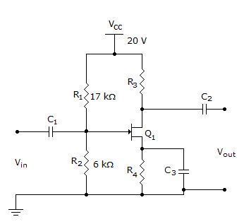
- A5.2 V
- B4.2 V
- C3.2 V
- D2.2 V
29The overall input capacitance of a dual-gate D-MOSFET is lower because the devices are usually connected:
- Ain parallel
- Bwith separate insulation
- Cwith separate inputs
- Din series
30What is the transconductance of an FET when delta ID = 1 mA and delta VGS = 1 V?
- A1 kS
- B1 mS
- C1 kiloohm
- D1 milliohm
31Which component is considered to be an "OFF" device?
- Atransistor
- BJFET
- CD-MOSFET
- DE-MOSFET
32In an n-channel JFET, what will happen at the pinch-off voltage?
- AThe value of VDS at which further increases in VDS will cause no further increases in ID.
- BThe value of VGS at which further decreases in VGS will cause no further increases in ID.
- CThe value of VDG at which further decreases in VDG will cause no further increases in ID.
- DThe value of VDS at which further increases in VGS will cause no further increases in ID
Information
- Description
- II Engineering Electronics II Quiz on Field Effect Transistors, created by Tony Mae on 06/03/2021.
- Author
- Tony Mae
- Language
- English
- Views
- 25
- Tags
- Rating
- No ratings yet Rate this quiz