
Flowchart
Untitled
Flowchart content
Digital Logic Circuits
A computer system has three main components: a central processing uni t (CPU) or processor, a memory unit , and input/outpu t (I/O) devices. Thes e three components are interconnected by a system bus.
The control bus consists of a set of control signals. Typica l control signals include memory read, memory write , I/O read, I/O write , interrupt , interrup t acknowledge, bus request, and bus grant.
The system memory, also called main memory or primary memory, is used to store both program instructions and data.
The system bus is the communication medium for data transfers. Such data transfers are called bus transactions
Every bus transaction involves a master and a slave
master is the initiator of the transaction
slave is the target of the transaction.
Simple Logic Gates
The gates are three basic logical operators: AND , OR, and NOT
A truth table is a list of all possible input combinations and their corresponding output.
is convenient to implement certain other gates,the NAND gate is equivalent to an AND gate followed by a NOT gate. Similarly, the NOR gates are a combination of the OR and NOT gates. The exclusive-OR (XOR) gate generates a 1 output whenever the two inputs differ.
Logic gates are in turn built using transistors.
Logic Functions
A logical function can be specified verbally .
The major problem with verbal specification is the imprecision and the scope for ambiguity.
We can make this specification precise by using a truth table. I n the truth table method, for each possible input combination, we specify the output value. The truth table method makes sense for logica l functions a s the alphabet consists o f only 0 and 1 .
The advantage o f the truth table method is that i t is precise, but The main problem with the truth table method is that it is cumbersome as the number of rows grows exponentially with the number of logical variables
We can also use logical expressions to specify a logical function. Logica l expressions use the dot, -h , and overbar to represent the AND, OR, and NOT operations, respectively.
A logic circuit designer may use all the three forms during the design o f a logic circuit. A simple circuit design involves the following steps:
Firs t we have to obtain the truth table from the input specifications.
W e do not wan t to implemen t the logica l expression derived in the las t step as i t often contains some redundancy, leading to an inefficient design . For this reason, we simplify the logical expression.
Then we derive a logical expression from the truth table.
I n the final step, we implement the simplified logica l expression. To express the implementation, we use the graphical notation.
Bubble Notation In large circuits, drawing inverters can be avoided by following wha t is known as the "bubble" notation. The use of the bubble notation simplifies the circuit diagrams.
Deriving Logical Expressions
We can write a logical expression from a truth table in one of two forms: sum-of-products (SOP) and product-of-sums (POS) form
In sum-of-products form, we specify the combination of inputs for which the output should be 1 .
In product-of-sums form, we specify the combinations of inputs for which the output should be 0.
is expressed as an and term. This is the product term as we use • to represent the AND operation.
. We essentially complement what we have done to obtain the sum-of-products expression. Here we look for rows that have a 0 output. Each such row input variable combination is expressed as an OR term.
Simplifying Logical Expressions
The sum-of-products an d product-of-sums logica l expressions can be used to come up with a crude implementation that uses only the AND, OR, and NOT gates.
how we can simplify the logical expressions obtained from truth tables. Our focus is on sum-of-products expressions. There are three basic techniques: the algebraic manipulation, Karnaugh map, and Quine-McCluskey methods.
Algebraic Manipulation
we use the Boolean algebra to manipulate logical expressions. We need Boolean identities to facilitate this manipulation
If there is only one version, we list it under the and version. We can transform a law from the and version to the or version by replacing each 1 with a 0, 0 with a 1 , + with a •, and • with a +. This relationship is called duality.
This method definitely requires good intuition, which often implie s that one needs experience to know i f the final form has been derived.
Karnaugh Map Method
This is a graphical method and is suitable for simplifying logical expressions with a small number of Boolean variables (typically six or less).
This method is preferred to the algebraic method as it takes the guesswork out of the simplification process
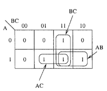
The basic idea behind this method is to label cells such that the neighboring cells differ in only one input bit position. This is the reason why the cells are labeled 00,01, 11 , 10 (notice the change in the order of the last two labels from the normal binary number order).
example how the maps are used to obtain minimal sum-of-products expressions for three-variable logica l expressions . Notic e tha t each cel l i s filled wit h the outpu t value o f the function corresponding to the input combination for that cell.
Combinational Circuits
One key characteristic of the circuits that we have designed so far is that the output of the circuit is a function of the inputs. Such devices are called combinational circuits as the output can be expressed as a combination of the inputs.
Higher-level abstraction helps the digital circuit design and implementation process in several ways. The most important ones are the following:
1. Higher-leve l abstraction helps us in the logica l design process as we can use functional building blocks that typically require several gates to implement. This , therefore, reduces the complexity.
2. Th e other equally importan t point is that the use of these higher-level functiona l devices reduces the chip count to implement a complex logical function.
Multiplexers
A multiplexer (MUX) is characterized by 2^ data inputs, n selection inputs, and a single output. The block diagram representation of a 4-input multiplexer (4-to-l multiplexer )
The multiplexer connects one of 2 ^ inputs, selected by the selection inputs, to the output.
we can implement any logical function using only multiplexers.
The best thing about using multiplexers is that you don't have to simplify the logical expression. We can proceed directly from the truth table to implementation, using the multiplexer as the building block.
How do we implement a truth table using the multiplexer? Simple . Connec t the logical variables in the logical expression as the selection inputs and the function outputs as constants to the data inputs.
Demultiplexers
The demultiplexer (DeMUX) performs the complementary operation of a multiplexer. A s in the multiplexer, a demultiplexer has n selection inputs.
However, the roles of data input and output are reversed. In a demultiplexer with n selection inputs, there are 2 '^ data outputs and one data input
Decoders
The decoder is another basic building block that is useful i n selecting one-out-of-A^ lines . The input to a decoder is an I-bit binary (i.e., encoded) number and the output is 2 ^ bits of decoded data.
Comparators
Comparators are useful fo r implementing relational operations such as =, <, > , and so on. For example, we can use XOR gates to test whether two numbers are equal.
Adders
We now look at adder circuits that provide the basic capability to perform arithmetic operations. The simplest of the adders is called a half-adder, which adds two bits and produces a sum and carry output
The problem with the half-adder is that we cannot use it to build adders that can add more than two 1-bit number
If we want to use the 1-bi t adder as a building block to construct larger adders that can add two A'^-bi t numbers, we need an adder that takes the two input bits and a potential carry generated by the previous bit position. This is what the full-adder does. A full adde r takes three bits and produces two outputs
If we want to improve the performance, we have to remove this dependency and determine the required carry-in for each bit position independently. Such adders are called carry lookahead adders. The main problem with these adders is that they are complex to implement for long words.
Programmable Logic Devices
Programmable Logic Arrays
(PLAs) PLA is a field programmable device to implement sum-of-product expressions
It consists of an AND array and an OR array, A PL A takes A ^ inputs and produces M outputs. Each input is a logical variable. Each output of a PLA represents a logical function output. Internally
each input is complemented, and a total of 2N input s is connected to each AND gate in the AND array through a fuse.
The OR array is organized similarly except that the inputs to the OR gates are the outputs of the AND array. Thus, the number of inputs to each OR gate is equal to the number of AND gates in the AND array. The output of each OR gate represents a function output.
Programmable Array Logic Devices (PALs)
PL As are very flexible in implementing sum-of-products expressions. However , the cost of providing a large number of fuses i s high.
We can reduce this complexity by noting that we can retain most of the flexibility by cutting down the set of fuses in the OR array. This is the rationale for PALs. Due to their cost advantage, most manufacturers produce only PALs.
PALs are very similar to PLAs except that there is no programmable OR array. Instead , the OR connections are fixed.
Arithmetic and Logic Units
The ALU forms the computational core of a processor, performing basic arithmetic and logical operations such as integer addition, subtraction, and logical AND and OR functions.
We use a multiplexer to select one of the four functions. Th e implementation is straightforward except that we implement the subtractor using a full adder by negating the B input.
To implement the subtract operation, we first convert B to — B in 2's complement representation. We get the 2's complement representation by complementing the bits and adding 1 . We need an inverter to complement. The required 1 i s added via C in.
Since the difference between the adder and subtracter is really the negation of the one input, we can get a better circuit by using a programmable inverter.
Remembe r that, when one of the inputs is one, the XOR gate acts as an inverter for the other input. W e can use these 1-bi t ALUs to get word-length ALUs.
Sequential Circuits
The output of a combinational circuit depends only on the current inputs. In contrast, the output of a sequential circuit depends both on the current input values as well as the past inputs. This dependence on past inputs gives the property of "memory" for sequential circuits.
Sometimes, this feedback consists of a simple interconnection of some outputs of the combinational circuit to its inputs. Fo r the most part, however, the feedback circui t consists of elements such as flip-flops tha t we discuss later.
System Clock
Digital circuits can operate in asynchronous or synchronous mode. Circuits that operate in asynchronous mode are independent of each other.
Asynchronous mode of operation causes serious problems in a typical digital system in which the output of one circuit goes as input to several others.
To avoid these problems, circuits are operated in synchronous mode. In this mode, all circuits in the system change their state at some precisely defined instants.
The clock signal provides such a global definition o f time instants at which changes can take place. Implici t in this definition is the fact that the clock signal also specifies the speed at which a circuit can operate.
The clock signal edge going from 0 to 1 is referred to as the rising edge (also called the positive or leading edge).
. The falling edge is also referred to as a negative or trailing edge.
Clock rate or frequency is measured in number of cycles per second. This number is referred to as Hertz (Hz). The clock period is defined as the time represented by one clock cycle.
Latches
It is time to look a t some simple sequential circuits that can remember a single bit value .
Latches are level-sensitive devices in that the device responds to the input signal levels (high or low). In contrast, flip-flops are edge-triggered.
SR Latch
The SR latch is the simplest of the sequential circuits that we consider. I t requires just two NOR gates. The feedback in this latch is a simple connection from the output of one NOR gate to the input of the other NOR gate
Clocked SR Latch
A basic problem with the SR latch is that the output follows the changes in the input. If we want to make the output respond to changes in the input at specific instants in order to synchronize with the rest of the system, we have to modify the circuit
The main change is that a clock input is used to gate the S and R inputs. These inputs are passed onto the original SR latch only when the clock signal is high. The inputs have no effect on the output when the clock signal is low.
D Latch
A problem with both versions of SR latches is that we have to avoid the SR = 11 inpu t combination. This problem is solved by the D latch
We use a single inverter to provide only complementary inputs at S and R inputs of the clocked SR latch . T o retain the value , we maintain the clock input at 0. The logic symbol and the truth table for the D latch clearly show that it can store a single bit.
Flip-Flops
We have noted that flip-flops are edge-triggered devices whereas latches are level sensitive. In the logic symbol, we use an arrowhead on the clock input to indicate a positive edge-triggered flip-flop
As is obvious from the bubble notation, we can convert a high level-sensitive latch to a low level-sensitive one by feeding the clock signal through an inverter
Similarly , we can invert the clock signal to change a negative edgetriggered flip-flop to a positive edge-triggered one.
Shift Registers
Shift registers , as the name suggests, shif t data left or right with each clock pulse.
built with positive edge-triggered JK flip-flops, shifts data to the right. For the first JK flip-flop, we need an inverter so that the K input is the complement of the data coming in ("Serial in" input).
Counters
We operate the JK flip-flops in the "toggle" mode with JK = 11 . The Q output of one flip-flop is connected as the clock input of the next flip-flop. The input clock, which drives our counter, is applied to FFO .
Counters are also useful in generating clocks with different frequencies by dividing the input clock.
ripple counter as the count bits ripple from the rightmost to the leftmost bi t (i.e., in our example, from FFO to FF2). A major problem with ripple counters is that they take a long time to propagate the count value.
We can design a counter in which all output bits change more or less at the same time. These are called synchronous counters. We can obtain a synchronous counter by manipulating the clock input to each flip-flop
TEC, sede central, Fundamentos de organizacion de computadoras
Escuela de Ingeniera en computacion
Resumen #6 (Sivarama - cap 2- Circuitos Logicos Digitales)
Jossy Mejia Vargas 2017109693
Lunes 11 de septiembre del 2017, 2 semestre, Esteban Arias Mendez
Information
- Description
- Flowchart on Untitled, created by Jossy Ivan Mejia Vargas on 12/09/2017.
- Created by
- Jossy Ivan Mejia Vargas
- Views
- 0
- Rating