
Mapa mental
SEMICONDUCTOR
Contenido del mapa
SEMICONDUCTOR
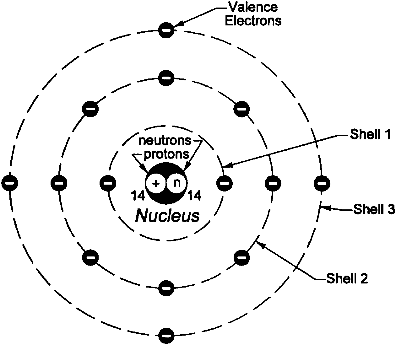
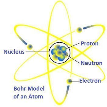
Bohr’s Atomic Theory
- •Central nucleus, surrounded by orbiting electrons.
- •Nucleus contains protons and neutrons.
- •Electrons orbit the nucleus.
- •Nucleus contains protons and neutrons.
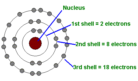
- The orbit paths of the electrons surrounding the nucleus are called shells.
- Each shell has a defined number of electrons it will hold (2n2).
- n=1, 2, 3, …..
- Example: Copper: 2.8.18.1 Electron valence: 1
- n=1, 2, 3, …..
- Each shell has a defined number of electrons it will hold (2n2).
- The outer shell is called the valence shell and electrons at this layer are called valence electrons.
- Maximum number of valence electron is 8.
- The material is more conductive if less electron valence orbiting the outer shell.
- Maximum number of valence electron is 8.
- •Central nucleus, surrounded by orbiting electrons.
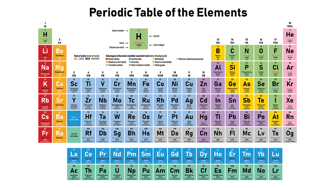
Periodic Table
Material Classification
- Conductor
- Low resistance which allows electrical current flow
- Charge flows freely
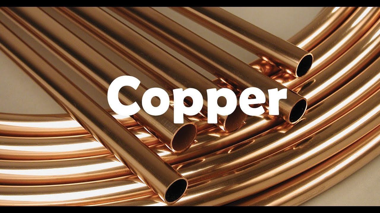
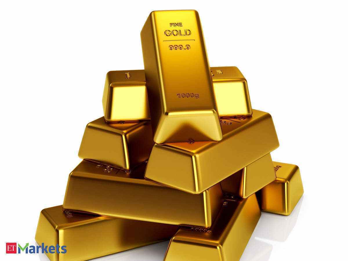
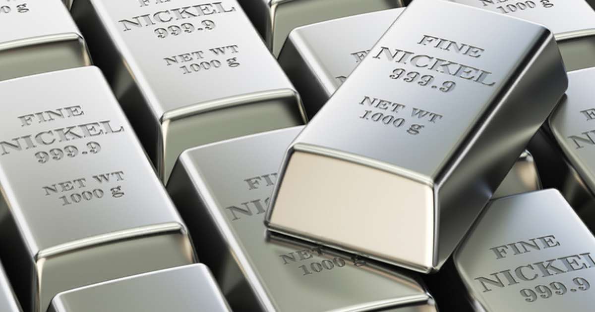
- Copper, silver, gold, aluminum, nickel etc.
- Insulator
- High resistance which suppresses electrical current flow
- Almost no charge flows
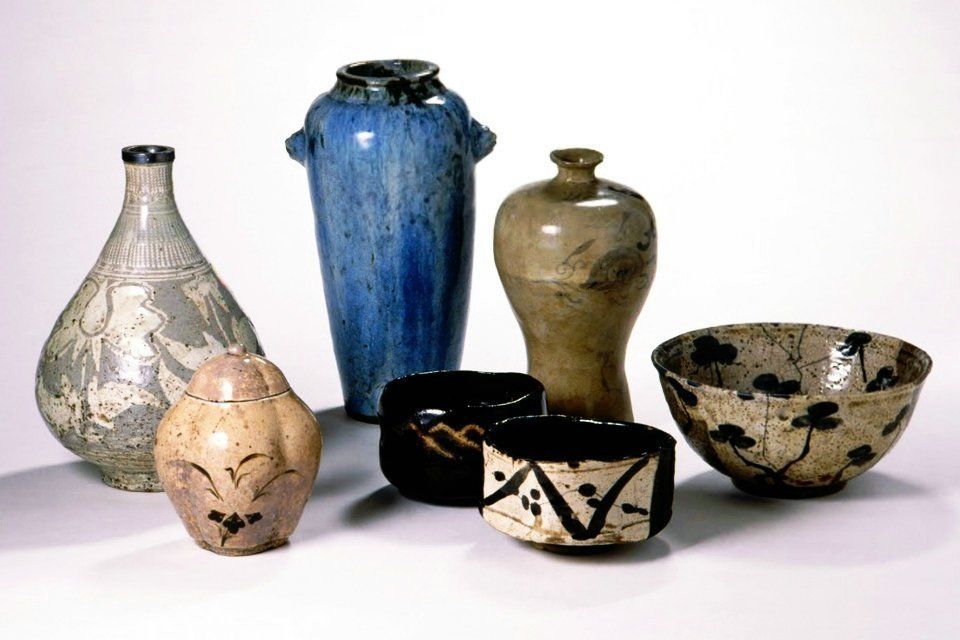
- Glass, ceramic, plastic, wood etc.
- Semiconductor
- Can allow or suppress electrical current flow
- Conductivity lies between conductor and insulator
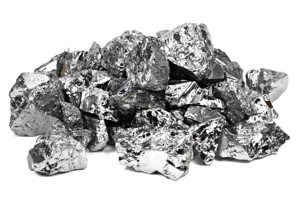
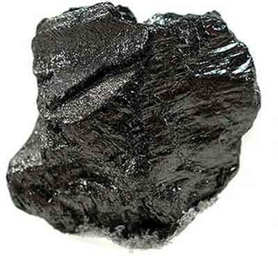
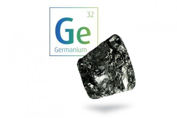
- Carbon, silicon, germanium etc.
- Conductor
Semiconductor
- Extrinsic
- Impuruties are added to improved semiconduvtivity
- Dopping Process
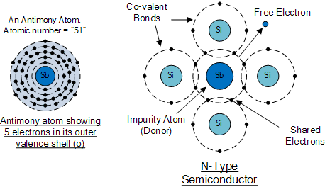
- N-type (Pentavalant)
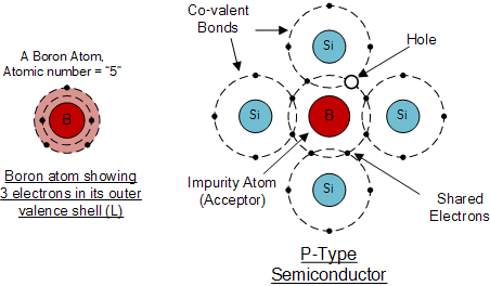
- P-type (Trivalant)
- Dopping Process
- Impuruties are added to improved semiconduvtivity
- Intrinsic
- Pure form of semiconductir
- Extrinsic
Energy Band
- Conductor
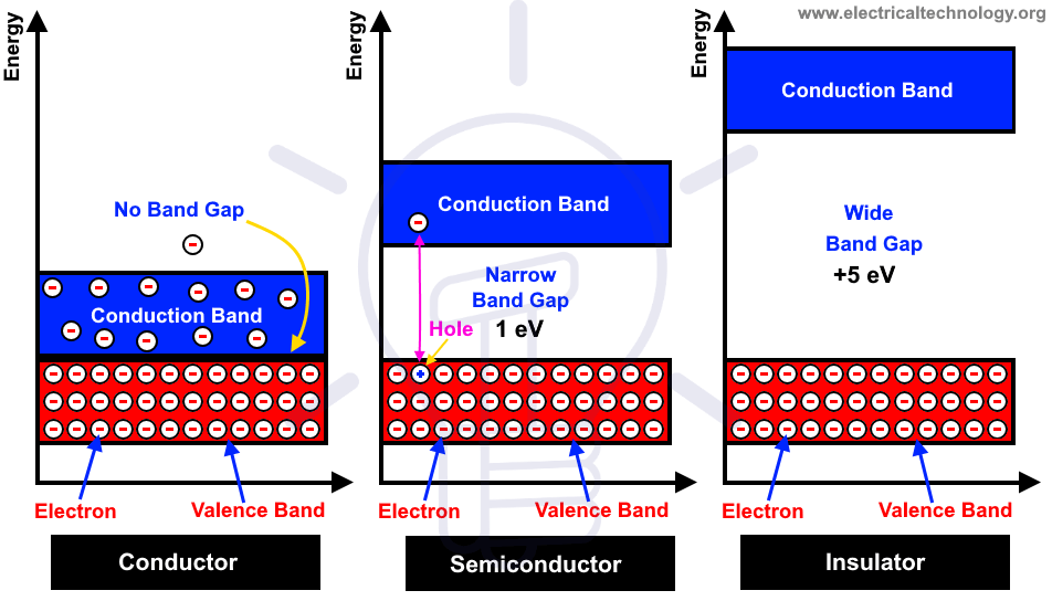
- Valence band – filled with electrons.
- Conduction band – empty.
- Band gap – empty.
- Electrons are unable to gain enough energy to jump from the valence band to the conduction band.
- Semiconductor
- Enables some electrons with enough energy to jump from the valence band to the conduction band easily.
- Temperature low – no free electron in the conduction band.
- Temperature high - electric conductivity high.
- When potential difference is connected, the holes and electrons move in opposite directions.
- Large number of electrons being excited into the conduction band, leaving a large number of holes in the valence band.
- Insulator
- Occupied by many conduction electrons, causing metal to become good electric conductor.
- Conductor
Imágenes y archivos del mapa


Información
- Descripción
- Mapa Mental sobre SEMICONDUCTOR, creado por SITI HATIPAH BT CHE MAT REDUAN el 10/11/2020.
- Creado por
- SITI HATIPAH BT CHE MAT REDUAN
- Visitas
- 3
- Valoración