Description
|
|
Created by andrew_nephin
almost 13 years ago
|
|
Page 1
Memory Mapping•uses the same address bus to access both memory and I/O devices ‒ the memory and registers of the I/O devices are mapped to (associated with) address values. •when an address is accessed by the CPU, it may refer to a portion of physical RAM, but it can also refer to memory of the I/O device. •the CPU instructions used to access the memory can also be used for accessing devices (simpler quicker code). • An address decoder monitors the CPU's address bus and enables the appropriate device allowing only one device to use the data bus at any instant (can be external or internal). To accommodate the I/O devices, areas of the address space used by the CPU must be reserved for I/O and must not be available for normal physical memory
von Neumann Architecture •Named after the mathematician and early computer scientist John von Neumann. • von Neumann machines have shared signals and memory for code and data. •Suitable for most general purpose CPUs since it is more flexible and easier to implement •Thus, the program can be easily modified by itself since it is stored in read-write memory.
Harvard Architecture •The name comes from the Harvard Mark I relay-based computer. •The most obvious characteristic of the Harvard Architecture is that it has physically separate signals and storage for code and data memory. •It is possible to access program memory and data memory simultaneously. •Typically, code (or program) memory is read-only and data memory is read-write. Therefore, it is impossible for program contents to be modified by the program itself.
Modified Harvard Architecture•Very much like a Harvard architecture machine, but it relaxes the strict separation between instruction and data while still letting the CPU concurrently access two (or more) memory buses. •The most common modification includes separate instruction and data caches backed by a common address space. –While the CPU executes from cache, it acts as a pure Harvard machine. –When accessing backing memory, it acts like a von Neumann machine (where code can be moved around like data, a powerful technique). •This modification is widespread in modern processors such as the ARM architecture. It is sometimes loosely called a Harvard architecture, overlooking the fact that it is actually "modified"
•What is the difference between a von Neumann architecture and a Harvard architecture–Harvard architecture has separate data and instruction busses, allowing transfers to be performed simultaneously on both busses. A Harvard architecture computer can thus be faster for a given circuit complexity because instruction fetches and data access do not contend for a single memory –Under pure von Neumann architecture the CPU can be either reading an instruction or reading/writing data from/to the memory. Both cannot occur at the same time since the instructions and data use the same bus system.
What’s the difference between MPU & MMU? An MMU is considered a more advanced device than an MPU. The features that are present in an MMU and not in the MPU include cache control, bus arbitration, and bank switching. The Memory Protection Unit prevents a user application from accessing memory regions own by OS. Memory Management Unit can do the same thing, but it also provide virtual memory (mapping of logical memory to a physical memory based on memory base offset defined by OS). In this way, a user program don't have to be loaded into a fix location in the main memory. It can be loaded and execute from anyway in the system memory, and the MMU can do the memory translation during program execution
Direct Memory Access (DMA)•The Cortex-M3 has an 8 channel DMA, each can be configured independently to handle a transfer from memory to memory, memory to peripheral, peripheral to memory peripheral to peripheral. •This movement of data by a separate DMA controller significantly reduces the load on the processor. •The DMA allows the CPU to be free for number crunching while it handles transfers by taking control of the bus, saving the cycles required if the CPU were to handle the transfer itself. • A DMA controller can save power in a system by putting the CPU in a low power state and using the DMA (fewer gates /transactions) to move the data. •Equally, using a DMA controller can achieve higher performance in a system where it moves data in parallel with processing in the CPU. •The DMA controller has a separate IRQ line that, when configured to so, interrupts when a transfer is complete.
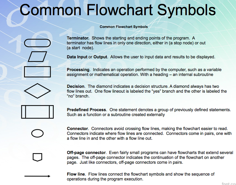
ALGORITHM•An algorithm is merely the sequence of steps taken to solve a problem –Two parts •Actions to be executed •Order in which those actions are to be done –Computational steps that transform the input data into useful output data. •Algorithms are not programs –They need to be coded in a programming language like C, C++, Basic or Assembley code.
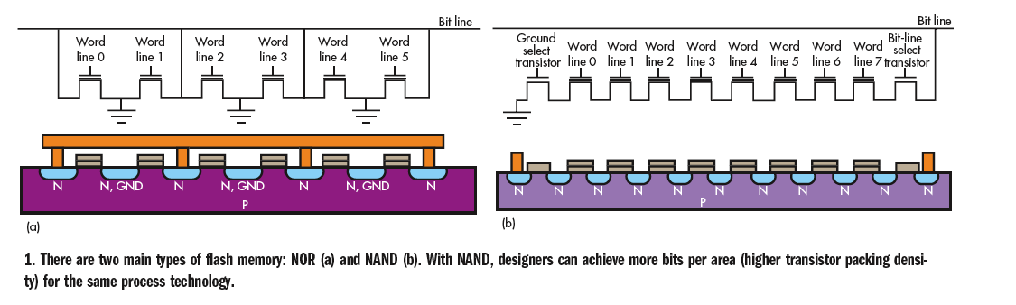
NAND flash memory is a type of non-volatile storage technology that does not require power to retain data. An important goal of NAND flash development has been to reduce the cost per bit and increase maximum chip capacity so that flash memory can compete with magnetic storage devices like hard disks. NAND flash has found a market in devices to which large files are frequently uploaded and replaced. MP3 players, digital cameras and USB drives use NAND flash. NAND has a finite number of write cycles. NAND failure is usually gradual as individual cells fail and overall performance degrades. To help compensate, some vendors over-subscribe their systems, by including more memory than is actually claimed. When a NAND card wears out, the user simply buys a new one, and the device continues to function. By passing the expense of additional storage on to the consumer, manufacturers have been able to lower the price of consumer electronic devices significantly. New developments in NAND flash memory technology are making the chips smaller, increasing the maximum read-write cycles and lowering voltage demands. Such improvements will continue make the technology even more common.
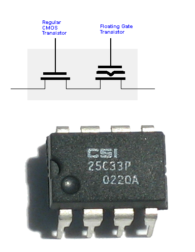
EEPROM (Electrically Erasable Programmable ROM) A rewritable memory chip that holds its content without power. EEPROMs are bit or byte addressable at the write level, which means either the bit or byte must be erased before it can be re-written. In flash memory, which evolved from EEPROMs and is almost identical in architecture, an entire block of bytes must be erased before writing. In addition, EEPROMs are typically used on circuit boards to store small amounts of instructions and data, whereas flash memory modules hold gigabytes of data for digital camera storage and hard disk replacements (see flash memory). A Floating Gate Holds the Charge EEPROM and flash memory bit cells are CMOS-based transistors that hold a charge on a "floating gate." With no charge on the floating gate, the transistor acts normally, and a pulse on the control gate causes current to flow. When charged, it blocks the control gate action, and current does not flow. Charging is accomplished by grounding the source and drain terminals and placing sufficient voltage on the control gate tunnel through the oxide to the floating gate. A reverse voltage channeled from another transistor clears the charge by causing it to dissipate into the substrate.
MEMORY
DMA
PROGRAMMING
Memory Devices
EEPROM
Want to create your own Notes for free with GoConqr? Learn more.