
Mind map
PCB manufacture
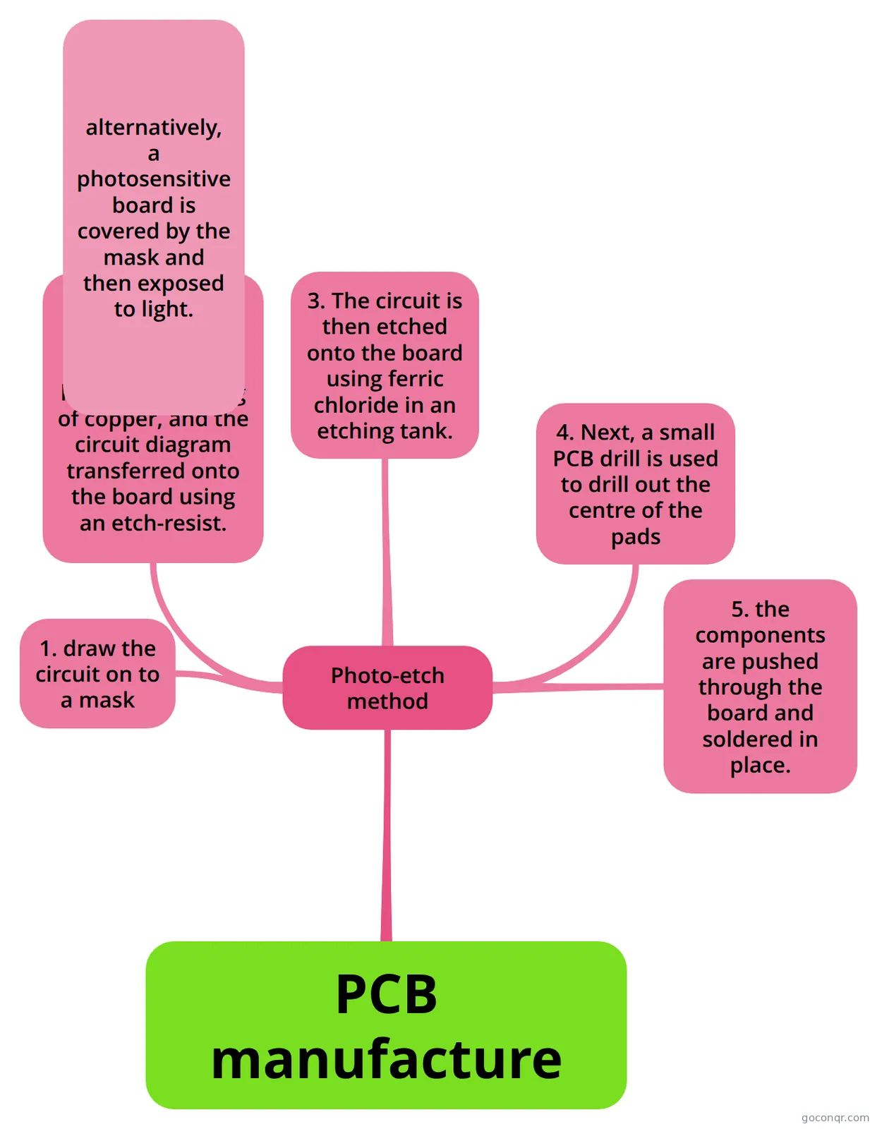
Mind map: PCB manufacture
Map content
PCB manufacture
Photo-etch method
- 1. draw the circuit on to a mask
- 2. The mask is then placed on the board, which has a thin coating of copper, and the circuit diagram transferred onto the board using an etch-resist.
- alternatively, a photosensitive board is covered by the mask and then exposed to light.
- 3. The circuit is then etched onto the board using ferric chloride in an etching tank.
- 4. Next, a small PCB drill is used to drill out the centre of the pads
- 5. the components are pushed through the board and soldered in place.
Information
- Description
- Electronics Mind Map on PCB manufacture, created by 08sarginson_re on 29/04/2013.
- Created by
- 08sarginson_re
- Views
- 211
- Tags
- Rating