
Fichas
Bipolar Junction Transistors
Fichas del conjunto (30)
- 1What is a transistor?An active component, its an amplifier. It has an external power supply which it uses to generate gain
- 2What happens to the base layer when a sufficient voltage is placed across it?Effectively disappears as it is so thin compared to the other layers
- 3Applying KCL to a transistor gives what equation?I(E) = I(C)+ I(B)
- 4What is another equation for I(C)?I(C) = I(C,majority) + I(CO)
- 5What is I(CO)?Collector current measured with the emitter open, is termed the LEAKAGE current
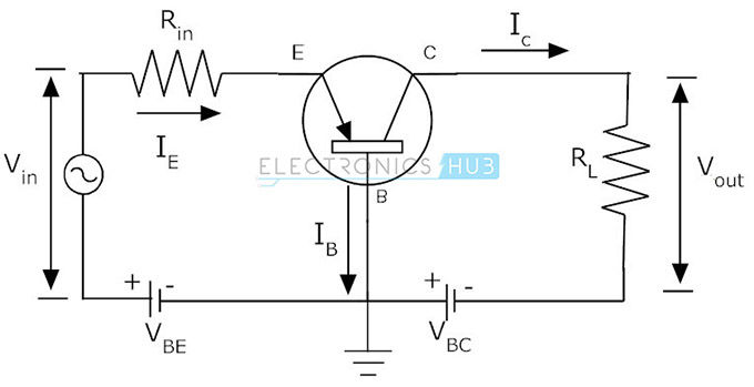
- 6What is the definition of "common base" configuration?The two voltage sources share the base terminal
- 7In the cut-off region what state are the junctions?Both are fully REVERSE bias
- 8In the saturation region what state are the junctions?Both are fully FORWARD bias
- 9What is ⍺(DC)?⍺(DC) = I(C) / I(E)
It's the common base short circuit amplification factor
Normally ranges from around 0.90 to 0.99, though the approximation is ⍺ = 1. - 10What is ⍺(AC)?⍺(AC) = ΔI(C) / ΔI(E)
The values of alpha are approximately equal for AC and DC - 11What is the definition of "common emitter" configuration?The two voltage sources share the emitter terminal
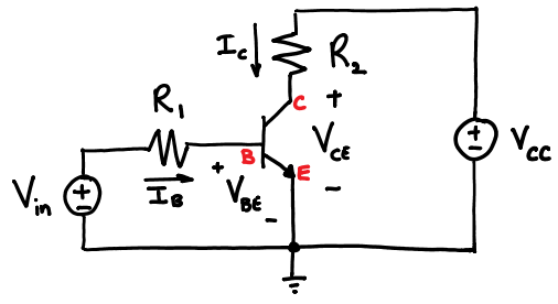
- 12How does common emitter vary from common base?The output characteristic lines of I(C) are much more sloped, the effect of the source used for gain is much greater
- 13What is β?β = I(C) / I(B)
Its the common-emitter forward amplification factor
Typically has a value between 50-400 - 14What is β often listed as on transistor data sheets?h(fe)
- 15How are ⍺ and β linked?β = ⍺ / (1 - ⍺)
⍺ = β / (β + 1) - 16What is the Quiescent point or 'Q' point?Refers to the DC biasing, so that the AC amplification occurs within the active region of the output characteristics
- 17What two currents does β link together?I(C) = β * I(B)
- 18What is the emitter current in a common emitter amplifier in terms of base current and β?I(E) = (1 + β) * I(B)
- 19What is the definition of a "common collector amplifier"
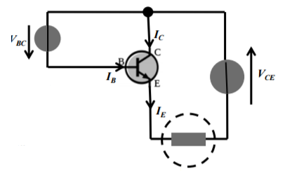
- 20What is the difference between common collector and common emitter?The output curves differ as I(E) = ⍺ * I(C)
- 21What limits the curves in the active region?Transistors have a maximum power dissipation so I(C) * V(CE) must be less than that value
- 22How to use derating info?It is used to calculate the max power when ambient air or case temperatures can't be met. As this value will be lower
- 23What are load lines?They are used to graphically solve problems where a non-linear circuit element is connected to a linear one
- 24What does a fixed bias transistor circuit look like?
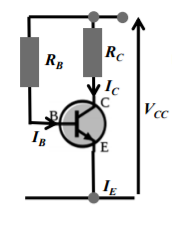
- 25What does a voltage divider bias transistor circuit look like?
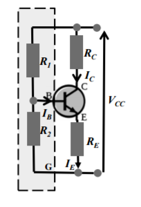
- 26What are the steps for finding bias voltages and currents?1. Simplify circuit for DC analysis
2. Simplify input using Thevenin's theorem
3. Calculate base current
4. Infer collector current
5. Calculate V(CE) from the 'load line' equation - 27What is the assumption given for the voltage across the emitter resistor?It is one tenth of the supply voltage
- 28What is the assumption made for the current through the potential divider and why is this assumption made?In order to maintain the bias, by maintaining I(B), the current through the potential divider must be greater than the base current. Say 10 times as an assumption
- 29What is the problem with class A amplifiers?Even when not amplifying the active device and series resistor(s) consume power. The theoretical efficiency is 50% at best
- 30What is linearity?The output increases exactly in proportion to the input. If this does not happen the signal is distorted, leading to harmonics.
Información
- Descripción
- (16ELA003 - Electronics) Engineering Fichas sobre Bipolar Junction Transistors, creado por Ben Evans el 18/04/2017.
- Creado por
- Ben Evans
- Visitas
- 18
- Valoración