
Mapa mental
ICT2104 Chapter 3: GPIO
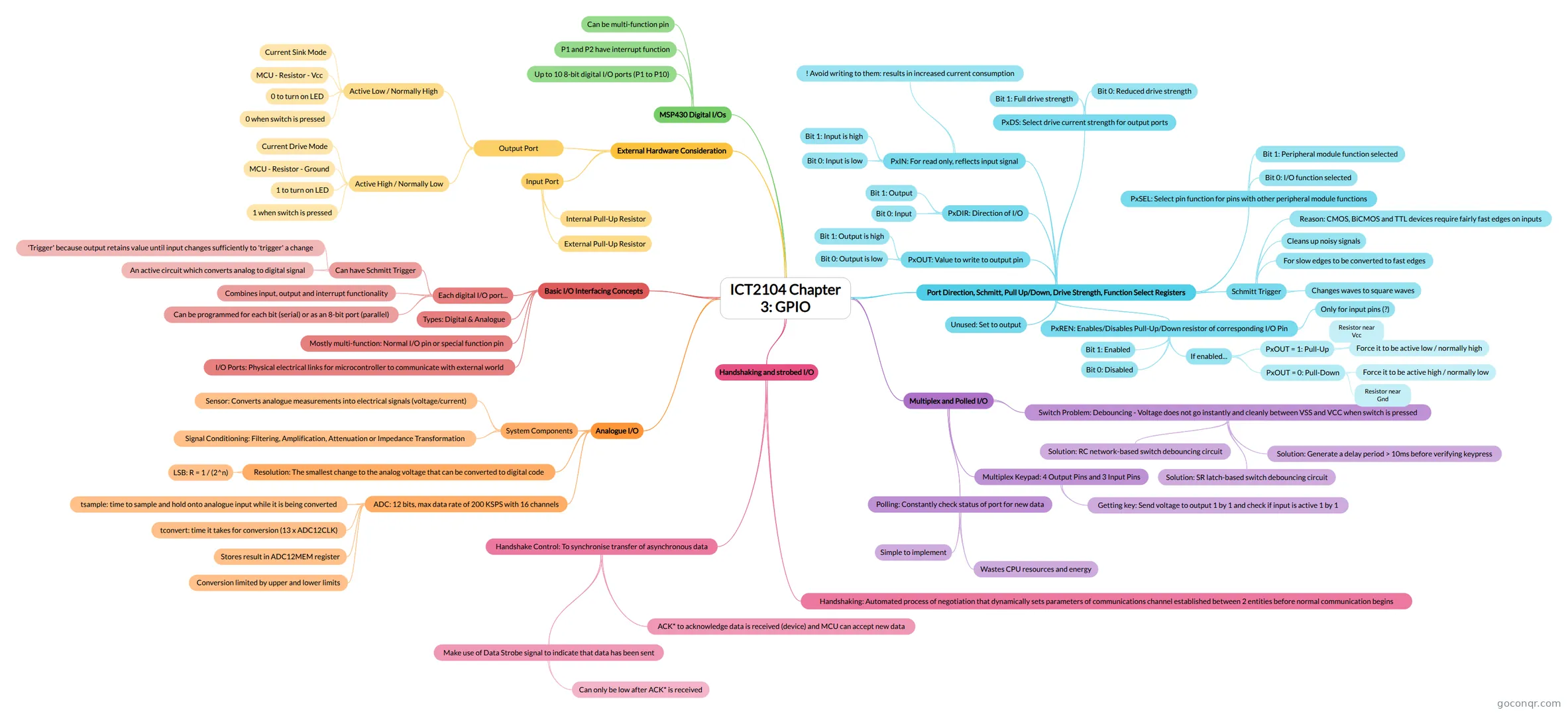
Mind map: MSP430 GPIO interfacing
Conteúdo do mapa
ICT2104 Chapter 3: GPIO
Basic I/O Interfacing Concepts
- I/O Ports: Physical electrical links for microcontroller to communicate with external world
- Types: Digital & Analogue
- Mostly multi-function: Normal I/O pin or special function pin
- Each digital I/O port...
- Can have Schmitt Trigger
- An active circuit which converts analog to digital signal
- 'Trigger' because output retains value until input changes sufficiently to 'trigger' a change
- Combines input, output and interrupt functionality
- Can be programmed for each bit (serial) or as an 8-bit port (parallel)
- Can have Schmitt Trigger
External Hardware Consideration
- Output Port
- Active Low / Normally High
- 0 to turn on LED
- 0 when switch is pressed
- MCU - Resistor - Vcc
- Current Sink Mode
- Active High / Normally Low
- 1 to turn on LED
- 1 when switch is pressed
- MCU - Resistor - Ground
- Current Drive Mode
- Active Low / Normally High
- Input Port
- External Pull-Up Resistor
- Internal Pull-Up Resistor
- Output Port
MSP430 Digital I/Os
- Up to 10 8-bit digital I/O ports (P1 to P10)
- P1 and P2 have interrupt function
- Can be multi-function pin
Port Direction, Schmitt, Pull Up/Down, Drive Strength, Function Select Registers
- PxDIR: Direction of I/O
- Bit 1: Output
- Bit 0: Input
- PxIN: For read only, reflects input signal
- Bit 1: Input is high
- Bit 0: Input is low
- ! Avoid writing to them: results in increased current consumption
- Schmitt Trigger
- For slow edges to be converted to fast edges
- Cleans up noisy signals
- Changes waves to square waves
- Reason: CMOS, BiCMOS and TTL devices require fairly fast edges on inputs
- PxOUT: Value to write to output pin
- Bit 1: Output is high
- Bit 0: Output is low
- PxREN: Enables/Disables Pull-Up/Down resistor of corresponding I/O Pin
- Bit 1: Enabled
- Bit 0: Disabled
- If enabled...
- PxOUT = 1: Pull-Up
- Force it to be active low / normally high
- Resistor near Vcc
- PxOUT = 0: Pull-Down
- Force it to be active high / normally low
- Resistor near Gnd
- PxOUT = 1: Pull-Up
- Only for input pins (?)
- PxDS: Select drive current strength for output ports
- Bit 1: Full drive strength
- Bit 0: Reduced drive strength
- PxSEL: Select pin function for pins with other peripheral module functions
- Bit 0: I/O function selected
- Bit 1: Peripheral module function selected
- Unused: Set to output
- PxDIR: Direction of I/O
Multiplex and Polled I/O
- Switch Problem: Debouncing - Voltage does not go instantly and cleanly between VSS and VCC when switch is pressed
- Solution: Generate a delay period > 10ms before verifying keypress
- Solution: SR latch-based switch debouncing circuit
- Solution: RC network-based switch debouncing circuit
- Multiplex Keypad: 4 Output Pins and 3 Input Pins
- Getting key: Send voltage to output 1 by 1 and check if input is active 1 by 1
- Polling: Constantly check status of port for new data
- Simple to implement
- Wastes CPU resources and energy
- Switch Problem: Debouncing - Voltage does not go instantly and cleanly between VSS and VCC when switch is pressed
Handshaking and strobed I/O
- Handshaking: Automated process of negotiation that dynamically sets parameters of communications channel established between 2 entities before normal communication begins
- Handshake Control: To synchronise transfer of asynchronous data
- Make use of Data Strobe signal to indicate that data has been sent
- Can only be low after ACK* is received
- ACK* to acknowledge data is received (device) and MCU can accept new data
- Make use of Data Strobe signal to indicate that data has been sent
Analogue I/O
- System Components
- Sensor: Converts analogue measurements into electrical signals (voltage/current)
- Signal Conditioning: Filtering, Amplification, Attenuation or Impedance Transformation
- Resolution: The smallest change to the analog voltage that can be converted to digital code
- LSB: R = 1 / (2^n)
- ADC: 12 bits, max data rate of 200 KSPS with 16 channels
- tsample: time to sample and hold onto analogue input while it is being converted
- tconvert: time it takes for conversion (13 x ADC12CLK)
- Stores result in ADC12MEM register
- Conversion limited by upper and lower limits
- System Components