
Karteikarten
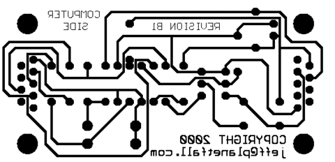
Electrical/Electronic processes
Karten in diesem Stapel (6)
- 1Stages of circuit board (PCB) manufacture- Designing the layout
- Producing the artwork
- PCB etching
- Drilling the board
- Populating the board and soldering - 2How do you design the PCB layout?- Usually designed using computer software.
- You draw tracks between components.
- Position components.
- Can also draw on paper or directly onto the board. - 3How do you produce the artwork?- If designed on a computer program print onto clear ACETATE
- 4PCB etching- By hand - Use a etch-resistant pen
- Photo etch board
- UV light box
- Developer solution
- Etching solution (ferric chloride) - 5PCB Etching process- Peel protective covering from board.
- Place artwork on the board.
- Place in the UV light box for 2 1/2 mins.
- Place board in developer solution, 10 secs.
- Place board in the ferric chloride.
- Rinse board with water. - 6—
Informationen
- Beschreibung
- BTEC Engineering Karteikarten am Electrical/Electronic processes, erstellt von Victoria Campbell am 22/01/2017.
- Erstellt von
- Victoria Campbell · Jan 2017
- Aktualisiert
- 22 Jan 2017
- Aufrufe
- 0
- Verlauf
-
- Erstellt von Ein gelöschter Nutzer · 6 Sep 2016
- Kopiert von Victoria Campbell · 22 Jan 2017
- Bewertung